 HOME > Research > Phase Change RAM
Phase Change RAM
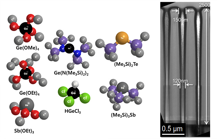
Ge-Sb-Te ALD process
The current PCRAM technology generally adopts a planar
structured (so called T-shaped) cell. However, further scaling is difficult
with a T-shaped cell due to the extremely low heating efficiency (only ~ 2 %)
of this structure. Plugging the PC material into a small contact hole (called
the confined cell structure) was suggested as the most efficient method to
improve the cell efficiency and increase the integration density. However, the
confined cell structure requires the PC material to be deposited with highly
conformal, reproducible, and rapid growth properties, which can usually be
accomplished by chemical vapor deposition (CVD) and atomic layer deposition
(ALD). However, the ALD of a PC material (most typically the Ge-Sb-Te
ternary material) is difficult because of the strong bond energy between the
metal ions (Ge, Sb and Te) and C as well as their covalent nature in most
common alkyl-based metal-organic precursors.
A genuine thermal ALD of Ge-Sb-Te phase changing material
layers at low temperatures (~ 70 oC), of which the composition lies
on the GeTe2 – Sb2Te3 tie line, is
realized using silyl-Te and alkoxy-Ge and alkoxy-Sb without the use of any
reaction gas. The strong affinity between the silyl group in the Te-precursor
and oxygen ions in the Ge- and Sb-precursors provide a fluent thermal ALD
reaction route to the system. This chemistry-specific ALD process was quite
robust against process variations resulting in highly conformal, smooth, and
reproducible film growth over a contact hole structure with an extreme
geometry.
Although the research group developed ALD of Ge-Sb-Te ternary
material, there were limitations in composition which lies on GeTe2-Sb2Te3
tie line. For various composition, novel Ge(II) precursors/silyl-Sb precursor
was suggested. As a result, stoichiometric GeTe and Sb-rich SbxTey
ALD were also developed. Thus, large area in Ge-Sb-Te ternary phase diagram can
be covered by combining these ALD processes with previously developed
processes.
Related Paper:
T Eom, et al., Chemistry of Materials, 11, 24,
2099 (2012)
T Eom, et al., Chemistry of Materials, 4, 26,
1583 (2014)
T Eom, et al., Chemistry of Materials, 10, 27,
3707 (2015)
T Eom, et al., Journal of Materials Chemistry C, 3, 1365
(2015)
PCRAM Cell Fabrication
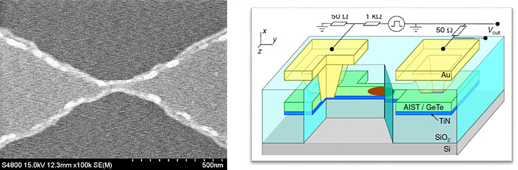
In order to evaluate/improve the electrical properties of
chalcogenide materials for PCRAM application, we design and fabricate various
cell geometries with e-beam lithography. The advantages of e-beam lithography
include high resolution of ~20nm and versatile pattern formations. We also
investigate different doping materials which can be applied to ALD and enhance
PCRAM device performances.
Ovonic Threshold Switch for Memory Selecotr Device
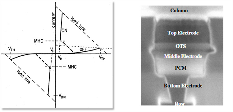
D. Adler, et al., Rev. Mod. Phys., 1978. D. C. Kau, et al., IEDM 2009
3D vertical cross-point array is a promising approach for
enabling next generation ultra-high density nonvolatile memory. However, the
implementation of resistive memory (e.g., RRAM and PCRAM) into dense
cross-point memory array must be addressed by a selector device with a strong
nonlinear IV characteristic in order to suppress sneak current paths.
Here, we focus on developing an ovonic threshold switch (OTS)
which is based on chalcogenide materials for memory selector application. Since
3D vertical architecture requires a deposition method with exceptional
conformity on high aspect ratio, we are interested in using atomic layer
deposition to achieve this goal.
Resistive Switching Behavior or Chalcogenide without Phase Change
Among the chalcogenide materials, alloys and compounds of Ge,
Sb and Te are one of the major materials for phase change memory (PCRAM.) The
applications such as a non-volatile memory entirely depend on the electrical
resistivity difference between crystalline and amorphous phase. This phase
change effect and consequent resistivity change by polarity-independent
electric pulse require high current density, which leads to high power
consumption issue that has been an obstacle for commercialization of PCRAM.
Chalcogenides play an important role as the electrolytes in
the electrochemical metallization (ECM) cell. Because the operation of the ECM
cell does not depend on the (local) melting and subsequent amorphization of the
chalcogenides, it does not require an excessively high reset switching from a
low-resistance state (LRS) to a high-resistance state (HRS) current, which was
the most significant problem in PCRAM. Nevertheless, the adoption of Ag or Cu
as the active metallic element could pose a problem such as contamination
issue. According to this concern, recent studies reported on the
chalcogenide-based ReRAM cell, wherein the conducting filament is comprised of
non-Cu element inside the chalcogenide alloys as a solid electrolyte.
Our research group focuses on polarity-dependent resistive
switching in amorphous Ge2Sb2Te5 (GST) thin
film by formation and rupture of Te-rich conducting filament, which does not
involve any phase change and thus can overcome demerits of conventional PCRAM.
Related paper:
Sijung Yoo et al., Nanoscale, 7, 6340-6347 (2015)