 HOME > Research > Oxide semiconductor TFT
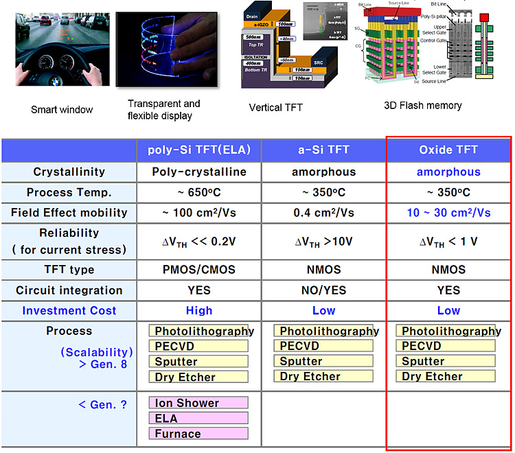
Oxide semiconductor TFT
Amorphous Oxide Semiconductor
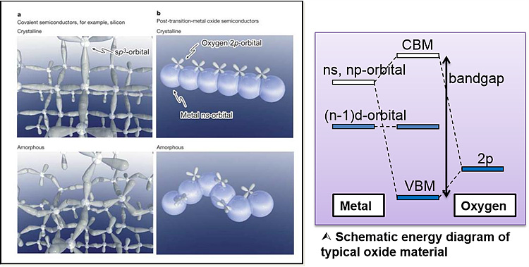
Since the discovery of the amorphous-InGaZnO (a-IGZO) by
Hideo Hosono in 2004, amorphous oxide semiconductors (AOS) have been attracting
great attention.
Ionic characteristics of oxides with two or more different
metal atoms (with different electronegativity) is strong enough that valence
band is formed by the oxygen 2p orbital and conduction band is formed by the ns
or np orbital of metal cation.
Oxides with large enough cations (n>4) have ns orbitals
that overlaps each other. Hence, oxides (i.e. IGZO) will have no directionality
in their conduction band and have high mobility even in the amorphous phase.
Relatively high mobility, transparency and low deposition
temperature has been the merits of amorphous oxide semiconductors. Due to these
merits, AOS materials are being used in display and memory devices.
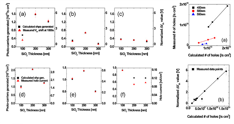
Gate Dielectric Effect on the NBITS (IGZO TFT)
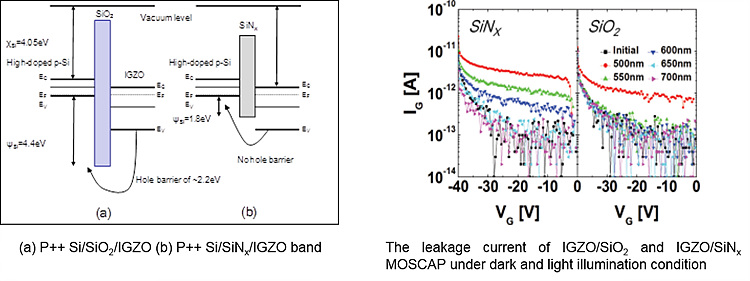
Hole current was directly observed in oxide semiconductors
under illumination. TFTs subjected to stress conditions in the dark and under
light illumination showed a negligible difference in Vth shift at wavelengths
longer than the threshold wavelength while a substantial difference was
observed at wavelengths shorter than it.
Hole trapping was found to be one of the reasons for the
NBITS instability in oxide semiconductor
Related paper:
Y. J. Chung, et al., Electrochemical and Solid-State
Letters, 6, 14, G35-G37 (2011)
J. H. Kim, et al., Applied Physics Letters, 23, 98,
232102 (2011)
J. H. Kim, et al., Physica Status Solidi Rapid Research Letters, 5-6, 5, 178-180 (2011)
Optical Modeling of Light Induced Phenomena in IGZO TFT
ITO/IGZO bilayer stacks in OTFT
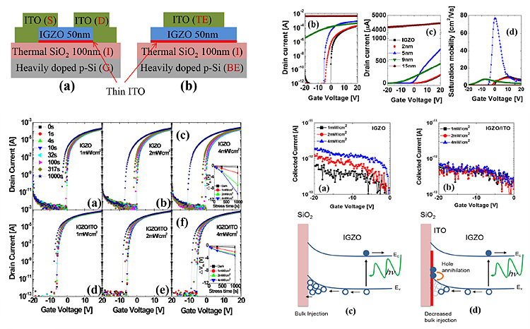
The optimized device portrayed a high saturation mobility of
~80 cm2/V s with off current values lower than 10-11A with 5nm ITO
at the gate dielectric / semiconductor interface. The negative bias
illumination conditions showed that a significant amount of ITO layer also
acted as a hole filter layer, and hole current and threshold voltage shift
values measured under photo-generated charge carriers were annihilated before
reaching the gate insulator.
Related paper:
Y. J. Chung, et al., Applied Physics Letters, 105, 013508
(2014)
Defect Analysis of AOS (ZTO)
The defects in AOS systems have been a major research topic
in the field because defects, especially oxygen vacancies, have a crucial
influence on the conductivity and device reliability. On that point, MOCVD
could be a viable method to fabricate the channel layer with better electrical
properties and lower defect concentrations compared to other deposition
methods. For these reasons, we investigated on physical, chemical, and
electrical properties of MOCVD ZnxSnyOz (ZTO)
thin films with various Zn/Sn atomic compositions.
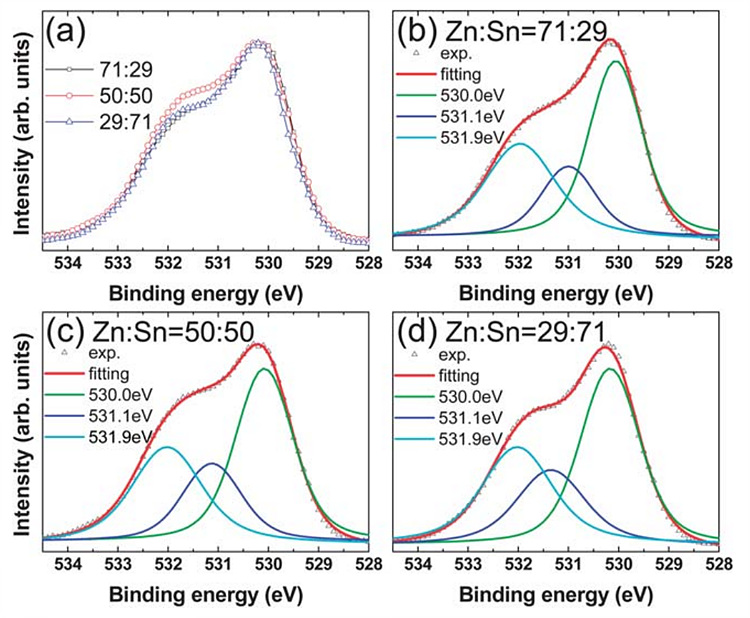
It is reported that free carriers are originated from the oxygen vacancies and carrier trapping occurs at the oxygen vacancies or at orbital states related to the oxygen vacancies. By varying composition, we observed that the relative area of the oxygen vacancy-related peak was changed and found out the relationship between the cation ratio and oxygen vacancy concentration.
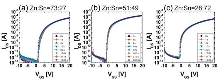
To examine the defect states and their influence on the
reliability, NBIS analysis was performed. Depending on composition of ZTO,
quite different electrical performances were shown. Applying NBIS stress for
1000 s, the transfer curves of the Zn-rich ZTO TFT showed a hump, but the
transfer curves of the Sn-rich ZTO TFT exhibited a parallel shift to the
negative bias direction. We determined these phenomena were attributed to the
difference in the oxygen vacancy energy states generated in the ZTO band gap by
light illumination.
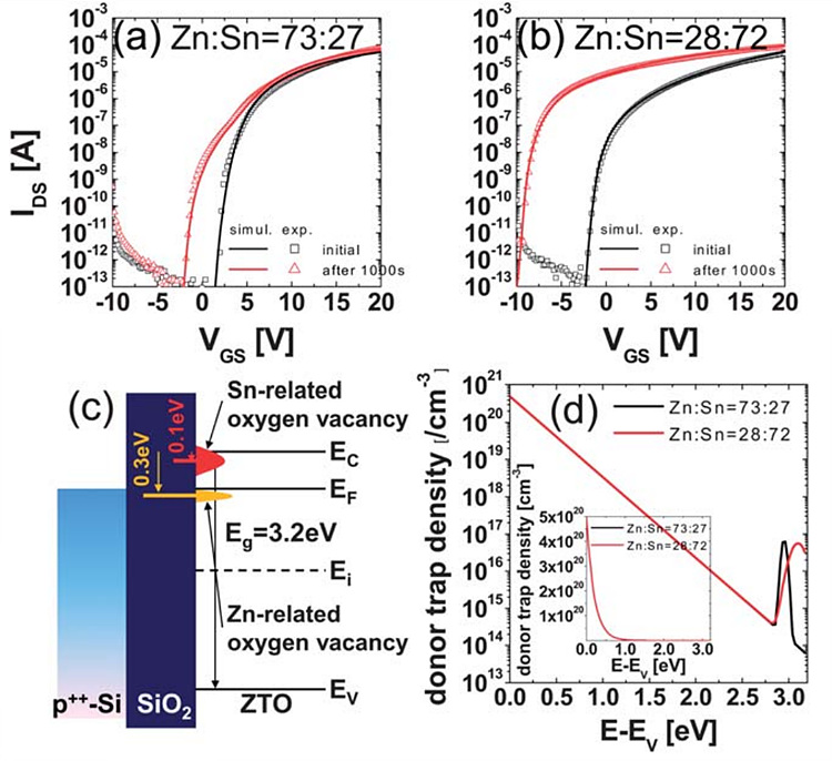
Recently, device simulation tool is widely used to understand
the experimental results or consider various possible factors. Using ATLAS
simulations on the transfer curves of the ZTO TFTs, we found that the Zn- and
Sn-related oxygen vacancies generated deep donor like trap states at 0.3 eV and
shallow states at 0.1 eV from the conduction band (or mobility) edge, which
induced the hump as well as shift and only parallel shift in the transfer
curves of the Zn-rich and Sn-rich films, respectively
Related Paper :
Un Ki Kim et al., J. Mater.
Chem. C, 1, 6695–6702 (2013)
P-type Tin Monooxide (SnO)
Since p-type oxide semiconductor materials with high enough
reliability are not reported yet, it is difficult to realize the complementary
circuit made from only oxide semiconductor materials. Thus, the research on the
p-type oxide materials has been recognized to be very important and valuable.
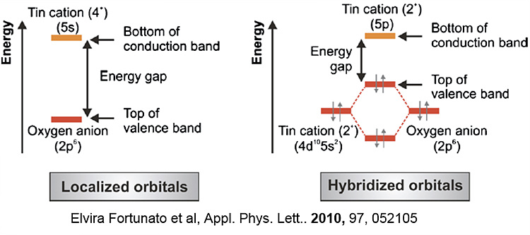
Among many candidates, tin monoxide (SnO) has received a lot
of attention as a p-type active layer because pseudo-closed Sn 5s and O 2p
orbitals having close energy levels for effective interaction.
They could form more isotropic and delocalized hybridized orbitals that would compose a VBM potentially giving more effective hole transport.
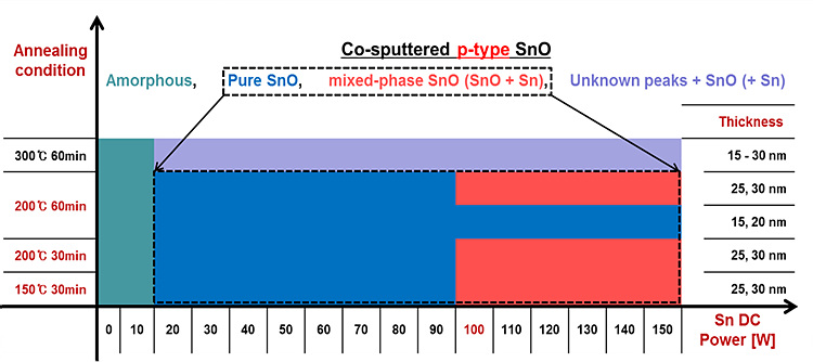
A wide range of process conditions for p-type SnO phase does exist.
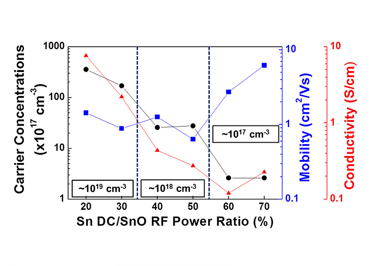
We have investigated the characteristics of p-type SnO thin films by co-sputtering technique with pure SnO and Sn targets. By controlling the co-sputtering conditions, p-type conductivity was observed in Hall-effect measurements. Deposited films exhibit a hole carrier concentration in the range of 3.1 1017 – 2.6 1023 cm-3; electrical conductivity between 0.266 – 9.91 103 S cm-1(see figure below); and Hall mobility around 10.3 cm2/V s at 50 % of Sn/SnO power ratio (The reported value is the average of 4–7 measurements performed on samples of every deposition condition). Among the various conditions of co-sputtering, the Sn-rich condition prevents oxidization from SnO to SnO2 and enhances the hole mobility due to valence band maximum (VBM) delocalization.
Electronic Structure of Crystalline and Amorphous ZnSnO3
Amorphous ZnSnOX is promising oxide semiconductor
of structural and electronic properties similar to those of IGZO. In
particular, ZnSnO3 (ZTO) is highly promising due to its
high mobility and easy fabrication. However, ZTO is less stable compared to
separated phases (Zn2SnO4+SnO2), so detailed
studies on its electronic structures and accompanied properties have been
limited. Especially, comparative studies on the detailed theoretical aspects of
electronic structures of the crystalline and amorphous ZTO are still lacking.
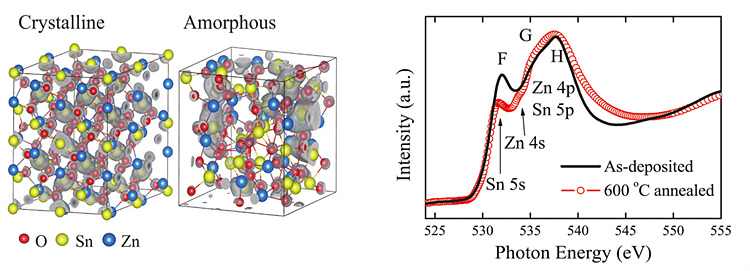
We theoretically investigated electronic structures of crystalline and
amorphous ZTO based on ab-initio calculations using Vienna ab-initio
simulation package (VASP) code. The results were compared with electronic
structure of ZTO films deposited by ALD technique and characterized by O K-edge
X-ray absorption spectroscopy (XAS). ab-initio calculation shows that
that the orbital character of the lowest CB was mostly Sn 5s for both phases.
However, the CB state was more localized for amorphous structure compared with
the crystalline case, although the degree of localization was not significant (left
figure). The difference in magnitude of localization of CB is also captured as
the difference in F-peak of XAS spectra between annealed (nano-crystalline) and
as-deposited (amorphous) ZTO films (right figure). The higher F-peak intensity
can be interpreted as a signature of strong Sn 5s localization in the
as-deposited sample, since O K-edge XAS reflects the unoccupied PDOS of the
metal ions that hybridize with the O 2p orbital states through the O
1s<->2p dipole transition.
Related Paper:
Property of Interface between ZnSnO3 and gate dielectric (SiO2)
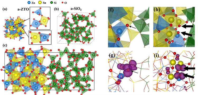
Compared to individual amorphous ZnSnO3 (a-ZTO)
and amorphous SiO2 (a-SiO2), information on
characteristic atomic structures arising at the interface between them and
associated electronic structures are quiet limited. For example, it has been well
known that atomic structure of bulk a-ZTO can be characterized by diverse
coordination numbers (CN=4~6) and polyhedral connectivities(corner, edge and
face-sharing) of M-O(M=Zn, Sn) polyhedra(fig. a) while that of a-SiO2
shows strict corner-shared Si-O tetrahedra(fig. b). However, it is important to
understand the interface properties in order to control and enhance the TFT
performance such as device stability. We simulated the eight interface
structures(a-ZTO/a-SiO2) using ab-initio molecular dynamics
simulation using VASP code (fig. c) and investigated atomic structure using
radial distribution function and electronic structure using PDOS. Atomic
structure at the interface features reduction of CN of M and O atoms consisting
of M-O polyhedra. It results in O-terminated M-O bonding (fig. f) and M-O-M
bonding (fig. h) structures where interfacial gap states consisting of O 2p
states appeared (fig. g and i). In contrast, CN of Si was nearly unchanged
indicating its strong tendency to form corner-sharing SiO4
tetrahedra as seen from its bulk structure, which we attribute to the reason of
reduction of CN of M and O atoms in M-O polyhedra. The result shows how the
differences in the coordination states and the connectivity of oxygen polyhedra
between a-ZTO and a-SiO2 play a role in bringing characteristic
atomic and electronic structures at the interface between them.
Related Paper:
J. Park, et al., Phys. Status Solidi B(accepted)