 HOME > Research > Phase Change Memory
Phase Change Memory
Phase change memory research
research overview
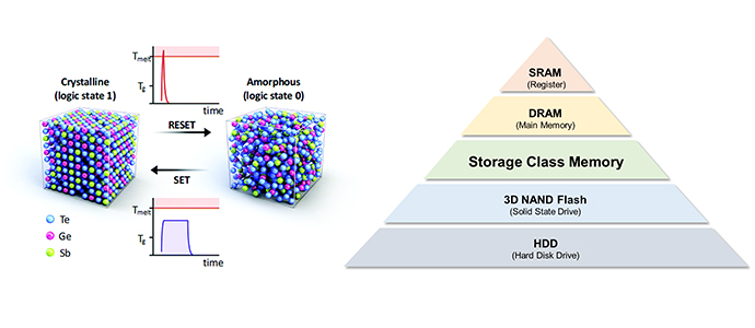
- Phase change memory (PCM) has been one of the most promising future memory devices. The non-volatility and fast operation of PCM expect to mitigate the performance gap between dynamic random access memory and nonvolatile NAND flash memory due to its fast programming, reasonable endurance, long data retention, and multilevel storage capability. PCMs are based on a chalcogenide material that can be quickly and reversibly switched between an amorphous (high-resistivity) and a crystalline (low-resistivity) phase with very different electrical properties. Set and reset state of PCM refers to low and high resistance states, respectively. The stored information is nonvolatile due to the stability of the phases, typically over 10 years at room temperature. The RESET process is performed by applying a large electrical pulse for a short time. The pulse allows amorphization of a particular region via melting and subsequent quenching. An opposite transition (SET) can be achieved by applying a smaller but longer electrical pulse to recrystallize the local amorphous region. An Ovonic threshold switch (OTS) refers to a chalcogenide-based selector device wherein the carrier generation-recombination, in conjunction with the lone pairs of the chalcogen ions, is responsible for the electrical thresholding behavior. The resistance switching is volatile because the process does not involve an amorphous to crystalline phase change, unlike in PCM.
Related Papers :
- Y K Lee et al. "Atomic layer deposition of chalcogenides for next-generation phase change memory." Journal of Materials Chemistry C, 9, 3708-3725 (2021).
1. Phase change memory
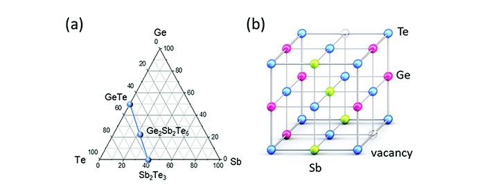
1-1) Ge-Sb-Te ALD process- The ALD of chalcogenides (which contain group-16 anions other than oxygen) has been motivated by their unique electrical switching behavior, which is desirable for memory and selector devices. For example, the ternary alloys of Ge-Sb-Te (GST) have become a main class of materials for phase-change memory (PCM). This is because of their facile electrical switching between the low- and high resistance states that can be driven by heating through a voltage pulse. Physical vapor deposition (PVD) is the conventional technique for depositing GST films in PCM. It was adopted for the first commercial PCM product by Intel-Micron (Optane). Nonetheless, its substitution by ALD has been pursued to overcome several problems of the current versions of PCM. For example, the two-dimensional crossbar structure of the current generation PCM requires high operation power and high fabrication costs. The confined or three-dimensional memory architectures enabled by ALD can decrease the high operating power and increase the limited integration density of PCM.
Related Papers :
- E Park et al. "Developing Precursor Chemistry for Atomic Layer Deposition of High-Density, Conformal GeTe Films for Phase-Change Memory." Chemistry of Materials, 31, 21, 8663-8772 (2019).
- E Park et al. "Atomic Layer Deposition of Nanocrystalline-As-Deposited (GeTe)x(Sb2Te3)1-x Films for Endurable Phase Change Memory." Chemistry of Materials, 31, 21, 8752-8763 (2019).
- Y K Lee et al. "Atomic layer deposition of chalcogenides for next-generation phase change memory." Journal of Materials Chemistry C, 9, 3708-3725 (2021).
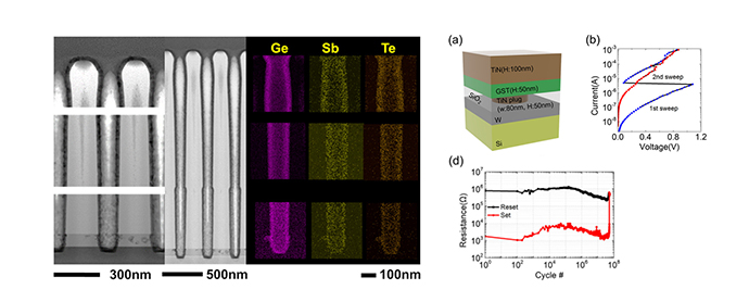
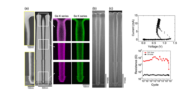
1-2) Vertical type memory fabrication
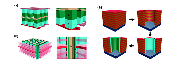
- Vertical-type structure of PCM was proposed to overcome the inherent limitations in the cost-effectiveness of the stacked planar architecture. The structure is motivated by the current vertical NAND flash memory design, which was proven to be highly efficient in achieving the large integration density of the memory over the terabit capacity. A phase-change film needs to be deposited conformally on the etched sidewalls in this vertical-type architecture. The high aspect ratio of the holes precludes the application of the PVD process. Considering the narrow hole diameter and its distribution over a large area, the ALD process becomes the most feasible method for the deposition of such conformal films, as described in a subsequent section. Since the fabrication of these vertical-type cells requires only a few lithography and patterning steps regardless of the number of layers, the fabrication cost increases only marginally with the integration density.
Related Papers :
- Y K Lee et al. "Atomic layer deposition of chalcogenides for next-generation phase change memory" Journal of Materials Chemistry C, 9, 3708-3725 (2021).
1-3) GeTe/Sb2Te3 superlattice ALD
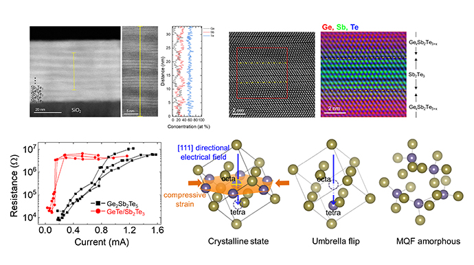
- This work demonstrates the development of the GeTe/Sb2Te3 superlattice film utilizing ALD (Atomic Layer Deposition) to achieve a high-performance PCM memory device. The peculiar chemical affinity of the ALD precursors to the substrate surface and the two-dimensional nature of the Sb2Te3 enabled the in-situ crystallized superlattice film where the out-of-plane directions of the two-component layers precisely matched the c-axis while the in-plane directions were random. The GeTe/Sb2Te3 superlattice film showed a RESET current of ~1/7 of randomly-oriented Ge2Sb2Te5 alloy film. The fluent improvement in the resistance switching performance from this GeTe/Sb2Te3 superlattice originates from the pressure-induced solid-state amorphization by the aligned superlattice film. This could be a step forward improvement for fabricating the futuristic PCM with low operating power, which may succeed in the current required SCM (Storage Class Memory).
2. Ovonic Threshold Switch for Selector Device
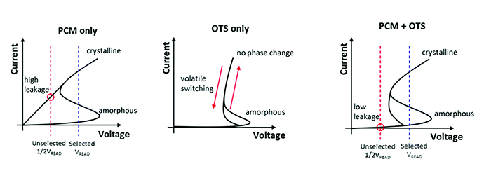
2-1) Ovonic Threshold Switch for Selector Device- A crossbar array of PCM offers a high integration density of cells with a two-terminal contact to a phase-change layer. The crossbar design requires a selector device to suppress the sneak current from unselected but low-resistance-state cells for accurate device operation. A selector device reduces an off-current (Ioff) flowing through the unselected cell by maintaining its high-resistance state under a small voltage bias. The upper figure schematically compares the I-V curves of the selected/unselected cells with and without a selector. An Ovonic threshold switch (OTS) refers to a chalcogenide-based selector device wherein the carrier generation-recombination, in conjunction with the lone pairs of the chalcogen ions, is responsible for the electrical threshold switching behavior. The resistance switching is volatile because the process does not involve an amorphous to crystalline phase change, unlike in PCM. The optimal compositions of OTS are different from those of PCM for this operation mode. The OTS device shows excellent properties, such as bidirectional operation, low Ioff, high Ion, high switching speed, and endurance. The ALD of various chalcogenides for the OTS has been pursued to deposit the films on various complex structures for the fabrication of large capacity PCM arrays in our research group, DTFL.
Related Papers :
- S Yoo*, C Yoo* et al. "Chemical interactions in the atomic layer deposition of Ge-Sb-Se-Te films and their ovonic threshold switching behavior." Journal of Materials Chemistry C, 6, 5025-5032 (2018).
- W Kim et al. "Atomic layer deposition of GeSe films using HGeCl3 and [(CH3)3Si]2Se with the discrete feeding method for the ovonic threshold switch." Nanotechnology, 29, 365202 (2018).
- C Yoo et al. "Atomic Layer Deposition of GexSe1-x Thin Films for Endurable Ovonic Threshold Selectors with a Low Threshold Voltage." ACS Applied Materials Interfaces, 12, 20, 23110-23118 (2020).
- Y K Lee et al. "Atomic layer deposition of chalcogenides for next-generation phase change memory." Journal of Materials Chemistry C, 9, 3708-3725 (2021)