 HOME > Research > Logic Devices
Logic Devices
Key-points for the next Goals
Metal gate
- - Increases gate controllability.
- - Fermi Level Pinning effect.
- - Vth tuning by effective work function.
High-k
- - Increases gate controllability
- - Allows use of thicker dielectric to reduce gate leakage.
High mobility channel
- - Increases channel mobility.
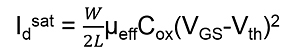
Logic device technology road-map
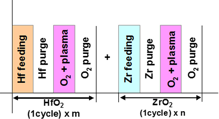
High-k oxide properties by ALD method
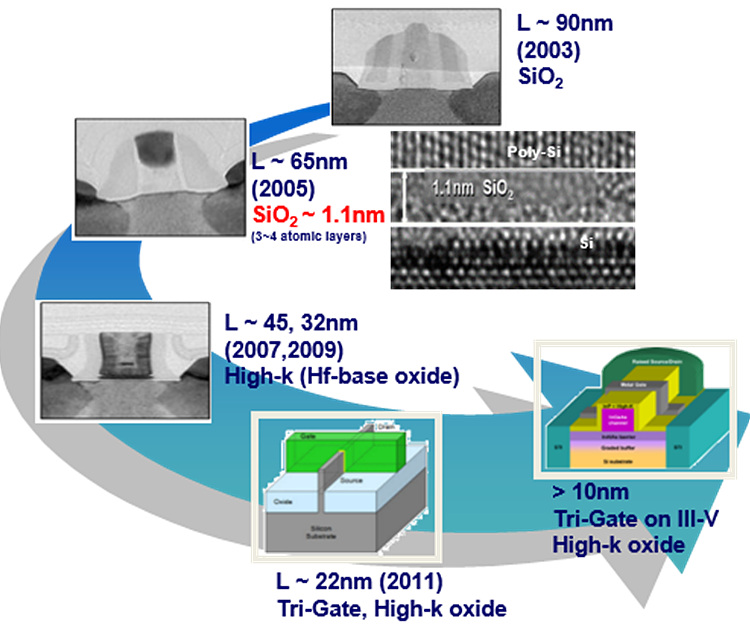
ALD Cycle structure
Related paper:
Lee, Jae Ho, et al. Journal of Vacuum Science & Technology B 32.3, 03D109 (2014)
Jung, Hyung-Suk, et al, Electron Devices, IEEE Transactions on 58.7, 2094-2103 (2011)
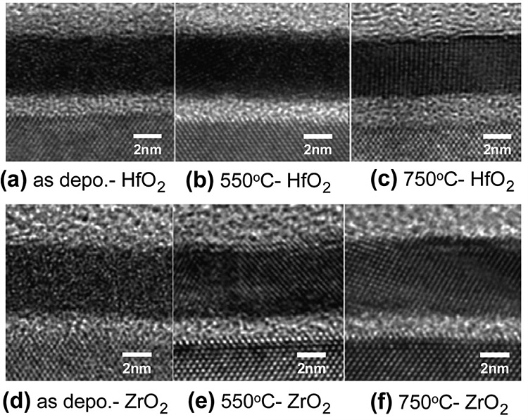
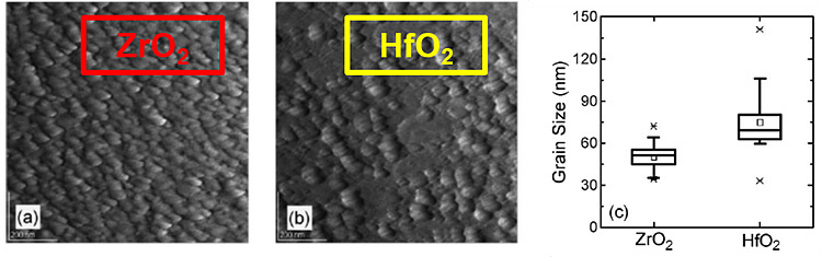
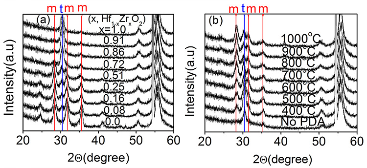
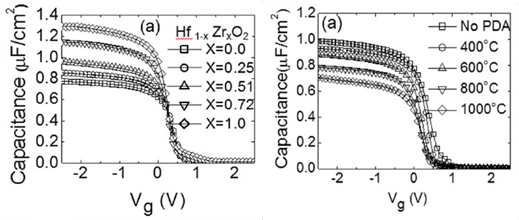
HfO2 based dielectrics for higher-k film
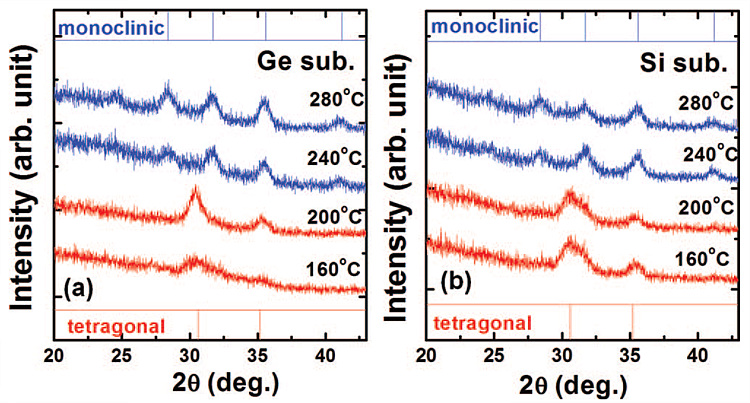
The high-dielectric-constant (high-k) HfO2 thin film became the industry-standard dielectric film for the highly scaled complementary metal insulator semiconductor field effect transistor (CMISFET) when the design rule reached 45nm. An efficient way of further increasing the k value of HfO2 is to transform its crystal structure from monoclinic (P21/c, k~17) to tetragonal {P4/nmc) or cubic phase (Fm3m), where the k values of both phase could be as high as 30-40. Tetragonal and cubic phase transition basically rely on the grain size effect (smaller grain size prefers the higher-k phase). One of the representative method for transformation of HfO2 to the higher-k phase is alloying with ZrO2 which has much smaller grain sizes than HfO2 film in ALD. An alloyed film named as Hf1-xZrxO2 (HZO) has shown various promising properties in terms of the k value and reliability considerations.
High Mobility Channel Materials
Although the first transistor was integrated on a Ge substrate
in the early 1960s, the absence of stable thermal Ge oxide has hindered the
wide use of Ge in complementary metal–oxide–semiconductor field-effect
transistor (CMOSFET) devices. Recently, significant advancements in the high-k
gate dielectric deposition have reemphasized Ge based devices. Moreover, a
Ge substrate is of particular interest for future CMOSFET devices because it
has higher electron (×2) and hole (×4) mobility compared to a Si substrate.
The atomic layer deposition (ALD) of high-k gate
dielectrics, most typically HfO2, on a Ge substrate has the potential to become
a mass-production-compatible process considering its matured process
technologies for mass production in the Si industry.
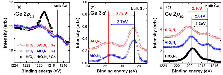
However, it is well known that, when high-k dielectrics are
deposited on a Ge substrate, they react with the substrate during the
deposition and postdeposition annealing (PDA) processes, which results in the
degradation of structural and electrical properties.
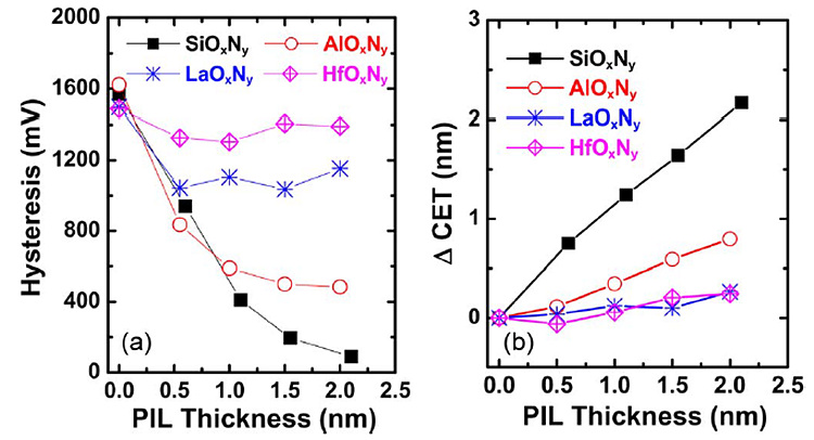
A typical example of this degradation is the very large capacitance-voltage (C–V ) hysteresis due to intermixing between dielectrics and the Ge substrate, which creates electrically active defects near the interface or in the bulk dielectrics films.
Ab initio modelling of High-K ALD on High mobility channel
Silicon has been used in most of the transistors for past 50
years due to the existence of a native oxide, SiO2. At the interface
of oxide/channel, there are interface traps which shift threshold voltage,
degrade channel mobility, and reduce Ion for a given Ioff
by trapping the electrons and holes. The native oxide of silicon meets the
requirements for the interface free of trapped charges. On the other hand, the
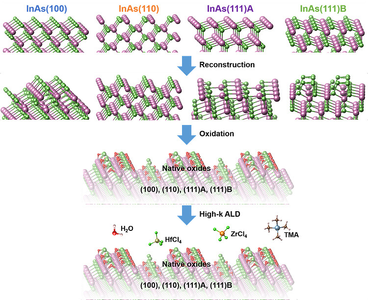
native oxide of Ⅲ-Ⅴ compounds easily result in the interface traps. The stable
oxide/Ⅲ-Ⅴ semiconductor interface is the most significant issue and the
interface with low density of interface traps is directly related to the
improved device performance.
Atomic layer deposition (ALD) is now used to fabricate thin
oxide films and enables to deposit high-k dielectrics on semiconductor
substrates. Especially, it was reported that native oxides of Ⅲ-Ⅴ semiconductor
is removed during early stage of ALD cycles. This is called ‘self-cleaning’ in
which organometallic precursors effectively reduce oxides covering substrates
and reduce interface traps. This indicates the possibility of high quality
oxide/ Ⅲ-Ⅴ interface.
To understand the interface trap generation mechanism during oxidation of Ⅲ-Ⅴ surfaces and chemistry of the self-cleaning effect, we use atomic-scale simulation in the frame of density functional theory (DFT). The ab-initio method can determine thermodynamic stability by calculating Gibbs free energy and kinetic priority by calculating rate constant of reaction.
Ab initio modelling of High-K Ge atomic structure
For the new-generation transistors using Ge-based channel
materials, the selection of the proper high-k materials and the control of the
interfacial layer are crucial in order to obtain the stable high-k/Ge
interface. However, germanium oxide interface generally shows considerably
higher defect concentrations relative to their silicon counterparts, which is
related to the low stability of GeO2 compared to SiO2.
DFT calculations provided the insight into the nature of typical defects
occurring at the Ge/GeOx interface, therefore with DFT calculation,
model structures of interface between Ge and GeOx is constructed. We
focus on the generation of transitional interface model. As the properties of
non-(100) surface become more important with the scaling-down of the devices,
interface structure with GeO2 and Ge(110) and (111) bulk structures
are also be considered.
To model the amorphous GeO2 structure in Ge/GeO2 stack, we choose to use molecular dynamics simulations, because this allows us to explore unexpected structural organizations. The a-GeO2 slab is generated from both a-quartz and rutile crystal. Mass density for a-GeO2 is set as the value in experiment (3.6g/cm3).
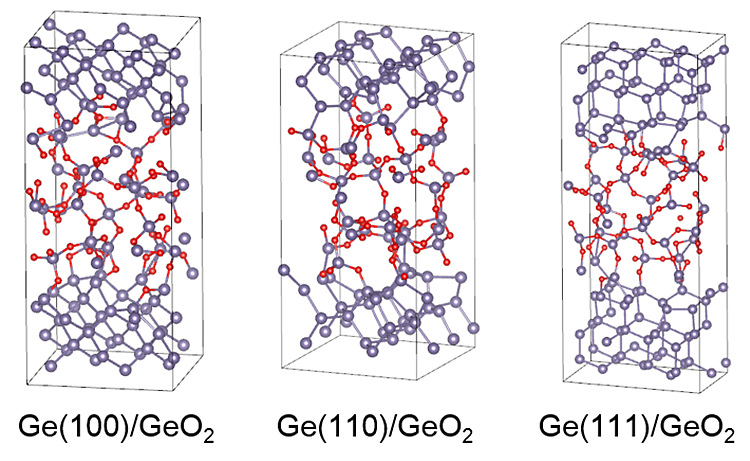
Ge/GeO2 Interface is constructed with ab-initio Molecular Dynamic simulation along with DFT calculation.
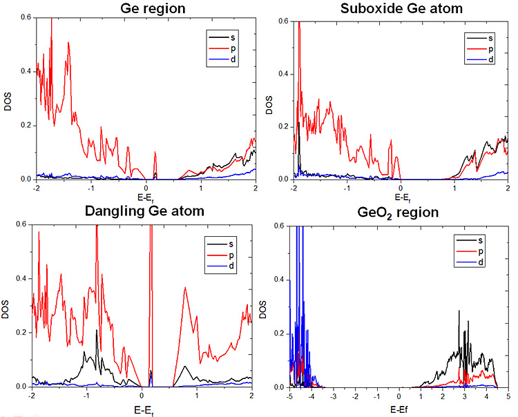
Ab-initio calculation on partial DOS of Ge atoms at Ge(100)/GeO2 interface.
For deeper exploration of interface atomic properties,
projected DOS for different types of Ge atoms were calculated with hybrid
functional calculation. Four types of Ge atoms are investigated: Ge atoms in Ge
region, Ge atoms at GeO2 region, well folded Ge atoms in suboxide
tetrahedron, and Ge atoms at defected sites.
It could be observed that the density states of suboxide Ge
atoms are similar with that of Ge region atoms. However, the dangling Ge atoms
would produce defect density states in the band gap of Ge atom. Therefore, the
defect sites in Ge/GeO2 interface could be treated as electrically
active defects, which is possible to alter the electronic properties of Ge
devices.