 HOME > Research > Dynamic RAM
Dynamic RAM
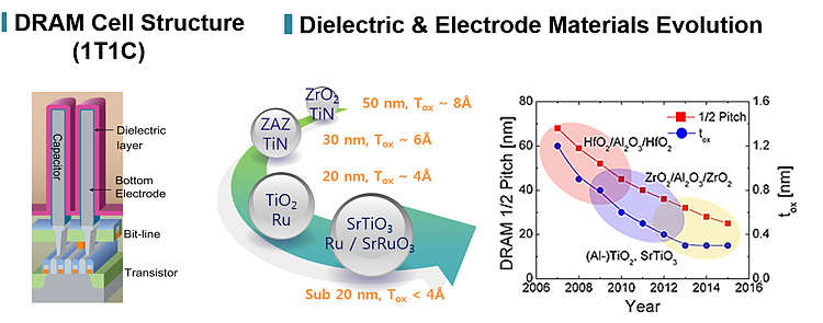
Recently, for sub 20nm scaled DRAM, capacitor structure has been changed to a metal-insulator-metal (MIM) structure in order to remove interfacial layers with low dielectric constant at the interface between polysilicon and dielectric material in SIS or MIS capacitors.
Due to the extremely small size of the capacitor, a three-dimensional structures such as trench hole/stack type are required for Gbit-scale DRAMs to obtain sufficient storage capacitance even though dielectrics with a high permittivity are used. Therefore, a ALD/CVD technique providing excellent conformality is required in order to fabricate the top and bottom electrodes as well as the dielectric films.
Ru and RuO2 are promising materials due to their good susceptibility to dry etching, low resistivity (Ru~7 μΩ-cm, RuO2~30 μΩ-cm), high chemical stability and high work function (Ru~4.7 eV, RuO2~5.1 eV) compared to the currently-used TiN electrode (~4.2 eV).
The use of rare earth ruthenium oxide materials, such as SrRuO3 (SRO), as electrodes or as interlayer between the electrode and high-k for ferroelectric and DRAM applications is mentioned in various roadmaps due to the good lattice matching with SrTiO3(STO) and relatively higher polarization property than elemental electrode.
Electrode materials for DRAM capacitors
Deposition of ALD-Ru Electrode with DER precursor
There are lots precursor for deposition of Ru film by ALD
method, such as Ru(EtCp)2, Ru(thd)2, etc. Among them, we have studied the
deposition method of Ru electrode with DER precursor
(2,4-(Dimethylpentadienyl)(ethylcyclopentadienyl)Ru) by ALD method using liquid
injection system(LDI). Unlike other conventional ALD system, such as
bubbler-type, LDI uses heated vaporizer. The precursor is injected to vaporizer
in liquid state and vaporized, then carrier gas deliver the vaporized precursor
into reaction chamber.
Pure and conformal Ru electrode films are deposited.
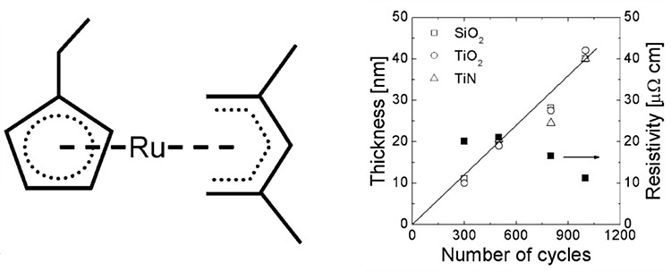
S. K. Kim et al, J.Electrochem.Soc., 154(2), 2007
Pulsed CVD growth of Ru/RuO2 with RuO4 precursor
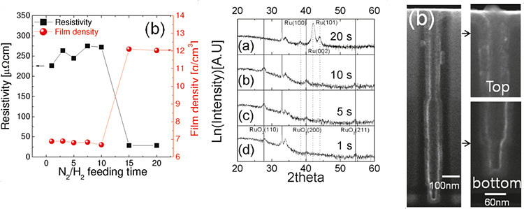
RuO4 precursor has very simple structure with
small molecular size, which makes it adoptable for deposition of Ru or RuO2
electrode films on complex-structured substrate. Over the temperature of 190ºC,
the RuO4 precursor is thermally decomposed to RuO2 phase
and self-limited growth behavior of ALD method is not shown. However, high
volatility of RuO4 molecule makes it possible that precursor
diffuses in short time and conformal film is deposited.
Phases of electrode films, Ru or RuO2, could be
controlled by injection time of H2-reduction gas, RuO2
for shorter H2 injection time and Ru for longer time. RuO2
films deposited by thermal decomposition of RuO4 precursor are
reduced to intermediate states, which are different with H2
injection time.
Related Paper:
J. H. Han, et al., Chem.Mater, 21.2, 2009
J. H. Han, et al., Chem.Mater, 22, 2010
J. H. Han, et al., Chem.Mater,
24.8, 2012
ALD growth of Ru electrode with RuO4 precursor
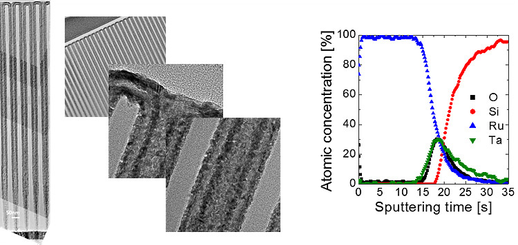
RuO4 precursor has been used for pulsed CVD growth
of Ru or RuO2 electrodes but ALD growth behavior is also shown at
low temperature. Under the decomposition temperature of RuO4
precursor, self-limited growth behavior which is a characteristic of ALD
deposition is observed. Deposited Ru electrode has low resistivity (~20μΩ-cm)
and low impurities.
ALD/CVD combined growth of SrRuO3
electrode
Strontium Ruthenate (SrRuO3, SRO) which has
perovskite structure and high work function value is being studied for
electrode materials for SrTiO3 dielectric film since it has good
lattice matching with STO film.
Deposition sequence of SRO electrode consists of few
subcycles that alternating ALD-SrO cycles and CVD-RuO2 cycles.
Generally, deposition of ternary system (oxide with two cations) is really
complicated since non-ideal ALD reactions could be shown between each layer. In
case of SRO, ALD-SrO layer shown initial excessive growth behavior due to
existence of RuO2 layer, which is not observed from the ALD method
of only SrO layer. Controlling excessive growth is very important since it
could degrade step coverage of electrode film. Improving the conformallity of
SRO film is being studied in several ways.
Related Paper:
J. H. Han, et al., Chem.Mater, 24, 2012
Dielectric materials for DRAM capacitors
The technology road map for memory devices states that tox(EOT, equivalent oxide thickness) less than 0.5nm is necessary for the DRAMs with a design rule of 20nm. It is also noted that there are no known material solutions to serve this purpose. Reducing the thickness of the dielectric films with k values ~20-30 to achieve the required tox results in unacceptably high leakage currents.
Among the various dielectric films, TiO2 thin
film in rutile phase exhibits a k value ~100 and therefore can be used for
DRAMs design rule. Moreover, Al ions as an acceptor can be doped into the TiO2 films
for decreasing the leakage current.
The ever-shrinking dimensions of DRAM cells with the
increasing packing density have made the capacitor size increasingly smaller
and currently-used ZrO2 dielectric will not be able to maintain
necessary capacitance. Some high-k dielectrics like SrTiO3 have
been avoided for dielectric materials of DRAM capacitors because of their
complicated structures and compositions, however, it is time to face the
difficulties and overcome them. (STO k~300, ZrO2 k~50)
Deposition of Al-doped TiO2 dielectric film with ALD method
TiO2 film has high dielectric constant, which
varies with the phase of TiO2, 40 for anatase phase and ~100 for
rutile phase. However, rutile phase with high dielectric constant is thermally
stable at high temperature over 800℃, which is such high temperature for
conventional ALD process.
Our group has reported that ALD-grown TiO2 film
with O3 has rutile phase on Ru or RuO2 substrate because
of formation of lattice-matching RuO2 interlayer. The coherence of
crystallinity induces the in-situ crystallization of TiO2 into
rutile phase.
Related Paper:
S. K. Kim, et al., Adv. Mater, 20, 2008
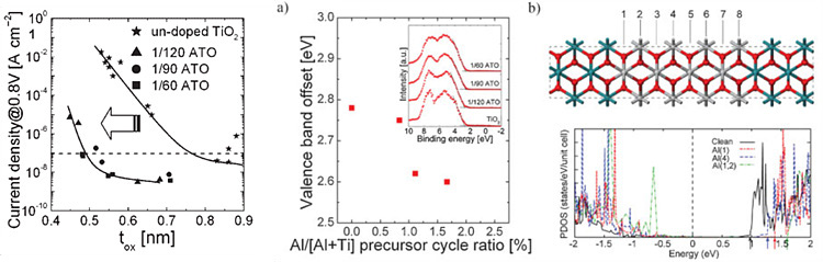
Rutile TiO2 film has dielectric constant but
higher leakage current is attended due to its small band gap(3.1eV) and n-type
nature. To suppress the leakage current characteristic, Al2O3
layer is inserted between TiO2 layers. Controlling the concentration
of Al atom varies the electrical characteristics. Doped Al atom which acts as
acceptor suppresses leakage current and lowers tox under 0.5nm.
Acceptor-like dopant Al atoms increases Schottky barrier
height(SBH) since the energy level of dopant site is under the oxygen vacancy
level of TiO2.
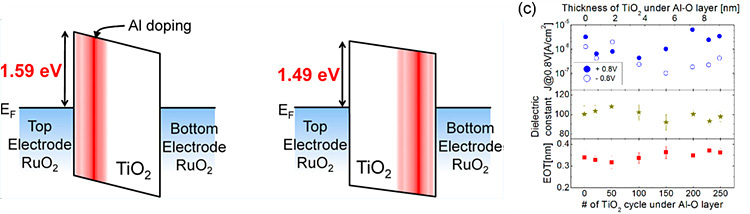
Position of Al2O3 layer in ATO film
also effects on electric characteristic of dielectric film. Lower leakage
current properties are shown when Al2O3 layer is inserted
near the electrode interface since leakage conduction mechanism of TiO2
film is Schottky emission conduction, which is sensitive to interface state.
Related Paper:
W. J. Jeon, et al., ACS Appl.Mater.Interfaces, 6(10),
2014
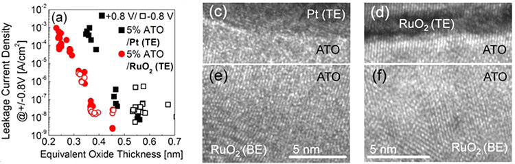
Further tox scaling of TiO2 under 0.4nm is achieved by adopting RuO2 top electrode in place of Pt top electrode. Just like the bottom electrode, RuO2 top electrode has structural coherence with TiO2 dielectric film and could reduce the tox of interface layer.
Related Paper:
W. J. Jeon, et al., ACS Appl.Mater.Interfaces, 6(23), 2014
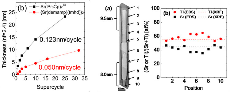
Deposition of ALD-SrTiO3 dielectric film and controlling growth behavior
SrTiO3 (STO) dielectric film, which has higher
dielectric constant, about 300, is also being studied for dielectric material
for next generation DRAM capacitor. ALD method depositing STO film consists of
several SrO cycles and TiO2 cycles. Those layers are deposited
alternatively and the sub-cycle ratio is varied to gain STO film with
stoichiometric cation ratio.
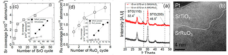
SrTiO3 film deposited on Ru substrate, which is a candidate of future DRAM electrode material, shows excessive growth of SrO layer since its oxygen-absorbing properties. The non-ideal excessive growth behavior could cause deviation of composition or thickness. Variation of the deposition process, such as temperature, precursor or inserting barrier layer has been studied for controlling growth behavior.
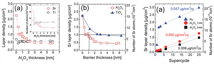
Related Paper:
W. Lee, et al., J. Mater. Chem, 22, 2012
Insertion of barrier layers like Al2O3 or TiO2 prevent the oxygen absorption of Sr precursor from oxidized Ru substrate. Barrier layers of certain thickness suppress the diffusion of oxygen atom and excessive growth is not shown. However, materials for barrier layer has lower dielectric constant than STO film so that net dielectric constant of capacitor decreases.
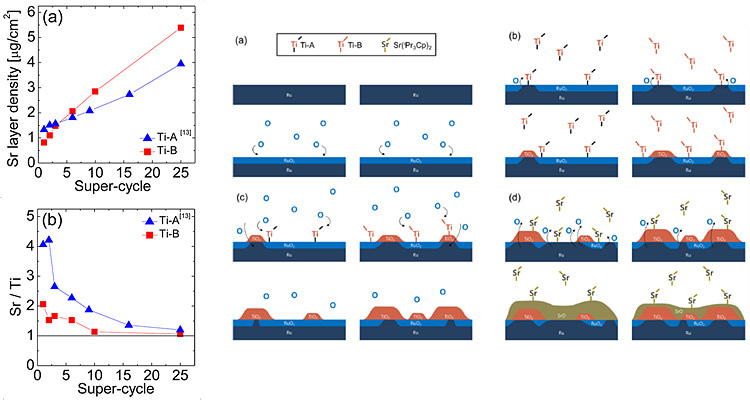
Related Paper:
W. Lee, et al., Chem. Mater, 25, 2013
Related Paper:
W. Lee, et al., Chem. Mater, 27, 2015
Variation of ALD precursor is another possibility for controlling growth behavior since the cause of non-ideal growth is the reaction between substrate-oxide layer or oxide-oxide layer. Using highly reactive precursor could enhance growth rate but excessive growth is also easily shown. Therefore, selecting proper precursor is important for ideal growth of STO film.
Ab initio modeling of perovskite hetero-interface (SrTiO3/LaAlO3&CaTiO3/LaAlO3)
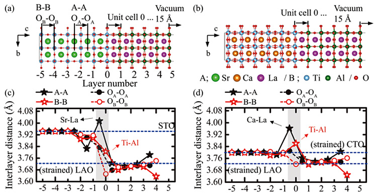
The recent growth techniques enabling the fabrication of the
oxide hetero-structures with atomically abrupt interfaces between dissimilar
materials allow us to investigate the physics of emerging phenomena arising at
the interface. One of the striking examples is the recent discovery of
two-dimensional electron gas (2DEG) at oxide interfaces: electrically
conducting layer is formed at the insulating LaAlO3 (LAO) and SrTiO3
(STO) interfaces. We investigated the symmetry-dependent interfacial
reconstruction from ab-initio calculations as a way of relieving the
polar discontinuity at the interface which may coexist with the 2DEG. As model
systems, we used the hetero-interfaces of LAO/STO and LAO/CTO, where the
crystal structure of STO is cubic while that of CTO is orthorhombic. We found
that only B-B interlayer distance increased at the LAO/STO(fig. c), while both
A-A and B-B interlayer distances increased at the LAO/CTO which corresponds to
the unit cell expansion at the interfacial region(fig. d). Moreover, the
octahedral tilt was found to play a crucial role for the interfacial reconstruction
and occurred in different ways depending on the crystal symmetry of the
materials that consist of the interface. Our finding provides an insight not only to understand the
fundamental physics of the emerging properties at the oxide interfaces but also
to design unique functional interfaces.
Related Paper:
J. Lee, et al. Appl. Phys. Lett. 106, 071601 (2015)