 HOME > Research > Thin Film Transistor
Thin Film Transistor
Thin-film transistor research
Amorphous Oxide Semiconductor
- Since the discovery of the amorphous-InGaZnO (a-IGZO) by Hideo Hosono in 2004, amorphous oxide semiconductors (AOS) have been attracting great attention.
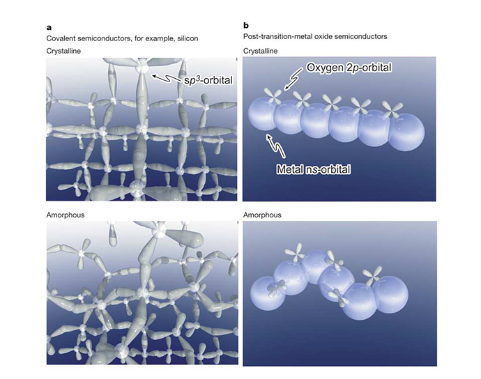
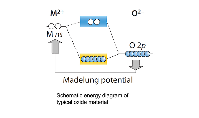
- Ionic characteristics of oxides with two or more different metal atoms (with different electronegativity) are strong enough that the valence band is formed by the oxygen 2p orbital, and the conduction band is formed by the ns or np orbital of metal cation.
- Oxides with large enough cations (n>4) have ns orbitals that overlap each other. Hence, oxides (i.e., IGZO) will have no directionality in their conduction band and have high mobility even in the amorphous phase.
- Relatively high mobility, transparency, and low deposition temperature have been the merits of amorphous oxide semiconductors. Due to these merits, AOS materials are being used in display and memory devices.
1. InGaZnO
1-1) Research on light-induced instability of a-IGZO TFTs- A-IGZO TFTs induce severe instability under negative bias temperature stress, reflecting the importance of studying the effect of light illumination on TFTs.
- Hole current was directly observed in oxide semiconductors under illumination. TFTs subjected to stress conditions in the dark and under light illumination showed a negligible difference in Vth shift at wavelengths longer than the threshold wavelength, while a substantial difference was observed at wavelengths shorter than it. Hole trapping was found to be one of the reasons for the NBITS instability in the oxide semiconductor.
- An optical model based on the transfer matrix method was used to predict the behavior of amorphous IGZO TFT and MOSCAP devices under illumination conditions. The simulation, considering the interference of light in the multi-layer structure, results well agree with experimental hole current and NBIS instability data. Such a method can be applied to any general system. With optical information of the films, results can be applied to minimize NBIS instability in an arbitrary AOS TFT for the display devices.
Related Papers :
- Y. J. Chung, et al. "Direct Observation of Hole Current in Amorphous Oxide Semiconductors under Illumination." Electrochemical and Solid-State Letters, 6, 14, G35-G37 (2011)
- J. H. Kim, et al. "Correlation of the change in transfer characteristics with the interfacial trap densities of amorphous In-Ga-Zn-O thin film transistors under light illumination." Applied Physics Letters, 23, 98, 232102 (2011)
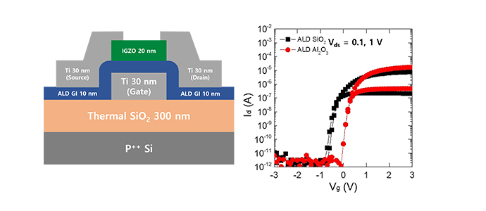
- J. H. Kim, et al. "Improvement in the negative bias illumination temperature stress instability of In-Ga-Zn-O thin film transistors using an Al2O3 buffer layer." Physica Status Solidi Rapid Research Letters, 5-6, 5, 178-180 (2011)
- Y. J. Chung, et al. "Optical modeling and experimental verification of light induced phenomena in In-Ga-Zn-O thin film transistors with varying gate insulator thickness." Journal of Applied Physics, 111, 024511 (2012)
- Y. J. Chung, et al. "Indium tin oxide/InGaZnO bilayer stacks for enhanced mobility and optical stability in amorphous oxide thin film transistors." Applied Physics Letters, 105, 013508 (2014)
Related research group email:
- jkim@hanbat.ac.kr - Prof. Jeong Hwan Kim
1-2) Application to charge trap device for NAND flash memory
- Recently, a-IGZO has attracted attention as a new channel material for the semiconductor memory applications, such as the vertically integrated NAND (V-NAND) flash memory devices. The present V-NAND adopts thin and poorly crystallized Si as the channel layer to minimize the cell-to-cell and device-to-device variability. However, the very low carrier (electron) mobility of such channel (<1 cm2 V-1s-1) deteriorates the device performance, which will eventually limit the maximum stackable number of device layers. Also, the limited critical dimension of the channel hole of the current V-NAND technology requires an alternative channel material that can improve its electrical characteristics without increasing its thickness. A-IGZO with higher mobility and uniformity in amorphous structure may be the viable solution for the next generation V-NAND technology.
Related Papers :
- Jung et al. "The charge trapping characteristics of Si3N4 and Al2O3 layers on amorphous-indium-gallium-zinc oxide thin films for memory application." Appl. Phys. Lett. 100, 183503 (2012)
- Rha et al. "Double-layered vertically integrated amorphous-In2Ga2ZnO7 thin-film transistor." Phys. Lett. 103, 183503 (2013)
- E. S. Hwang et al. "In2Ga2ZnO7 oxide semiconductor based charge trap device for NAND flash memory." Nanotechnology, 29, 155203 (11pp) (2018)
1-3) Application to DRAM cell transistor
- Currently, DRAM devices are facing the well-known “memory wall”, i.e., the speed discrepancy between the CPU and the memory located outside the CPU. 3D integration is a breakthrough in reducing this mismatch. However, the need for a storage capacitor limits the scalability of 3D DRAM cells. DRAM scaling is also limited by the steady increase of transistors off-current induced by the cell size reduction, as maintaining the current refresh time of 64 ms becomes challenging. InGaZnO4-based thin-film transistors (IGZO-TFTs) are very well known for their very low IOFF (<10-22A/μm), representing a solution for reducing the DRAM cell leakage. Despite the IGZO channel being commonly used in the amorphous phase, IGZO-TFTs show a high on/off ratio due to its unique band structure.
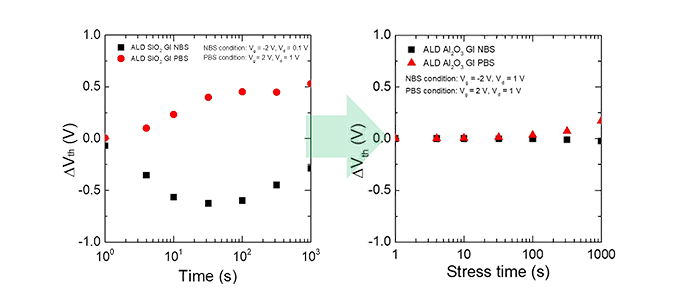
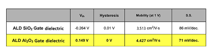
- Also, the electrical performance of IGZO TFTs is suitable for DRAM cell transistors. As shown above, IGZO TFTs show a very low subthreshold swing value (S.S.) close to the theoretical limit (60 mV/dec). In addition, when continuous bias stress is applied, there is no threshold voltage shift. Therefore, IGZO-TFTs are promising and reliable devices for DRAM cell transistors.
2. ZTO
2-1) Electronic Structure of Crystalline and Amorphous ZnSnO3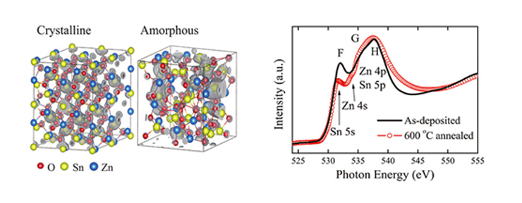
- We theoretically investigated electronic structures of crystalline and amorphous ZTO based on ab-initio calculations using the Vienna ab-initio simulation package (VASP) code. The results were compared with the electronic structure of ZTO films deposited by ALD technique and characterized by O K-edge X-ray absorption spectroscopy (XAS). ab-initio calculation shows that the orbital character of the lowest CB was mostly Sn 5s for both phases. However, the CB state was more localized for the amorphous structure compared with the crystalline case, although the degree of localization was not significant (left figure), reflects the unoccupied PDOS of the metal ions that hybridize with the O 2p orbital states through the O 1s<->2p dipole transition.
Related Paper :
- J. Lee, et al. "Ab initio study on the structural characteristics of amorphous Zn2SnO4." Appl. Phys. Lett. 102, 242111 (2013).
- J. Park, et al. "Atomic and electronic structures of a-ZnSnO3/a-SiO2 interface by ab initio molecular dynamics simulations." Physica Status Solidi B, 9, 253, 1765-1770 (2016).
2-2) Characteristics of ZTO TFTs depending on Zn/Sn ratio
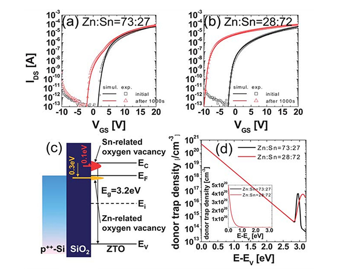
- It is reported that free carriers originated from the oxygen vacancies, and carrier trapping occurs at the oxygen vacancies or orbital states related to the oxygen vacancies. By varying composition, we observed that the relative area of the oxygen vacancy-related peak was changed and figured out the relationship between the cation ratio and oxygen vacancy concentration.
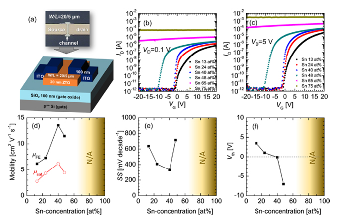
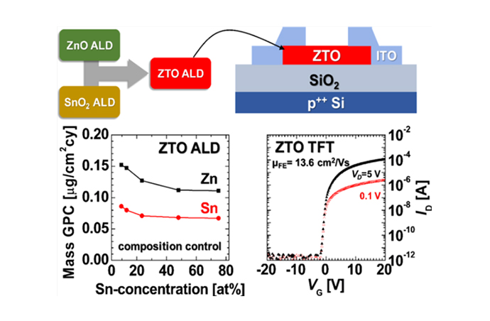
- When it comes to the ALD process, a significant incubation stage was observed for ZnO ALD on the Si substrate but not for the SnO2 thin-film substrate. The incubation cycles, along with the grain size, were increased with O3 feeding time, implying that the reactivity of the Zn-precursor varied with the degree of oxidation of the Si surface. The adsorption of the Zn-precursor in the early stage of (Zn,Sn)Ox ALD was facilitated with an increasing concentration ratio of Sn to Zn. A negative shift of threshold voltage occurred as the Sn-concentration increased in (Zn,Sn)Ox films. The best electrical performance of the oxide TFTs was observed when the Sn-concentration was 40 at %. The amorphous structure of the films could be retained up to 600 °C of post-annealing.
Related Papers :
- Un Ki Kim et al. "Study on the defects in metal-organic chemical vapor deposited zinc tin oxide thin films using negative bias illumination stability analysis." J. Mater. Chem. C, 1, 6695-6702 (2013)
- J. S. Kim, et al. "Substrate-Dependent Growth Behavior of Atomic-Layer-Deposited Zinc Oxide and Zinc Tin Oxide Thin Films for Thin-Film Transistor Applications." J. Phys. Chem. C, 2020, 124, 49, 26780-26792
2-3) Charge Trap Flash with ZnSnO channel layers
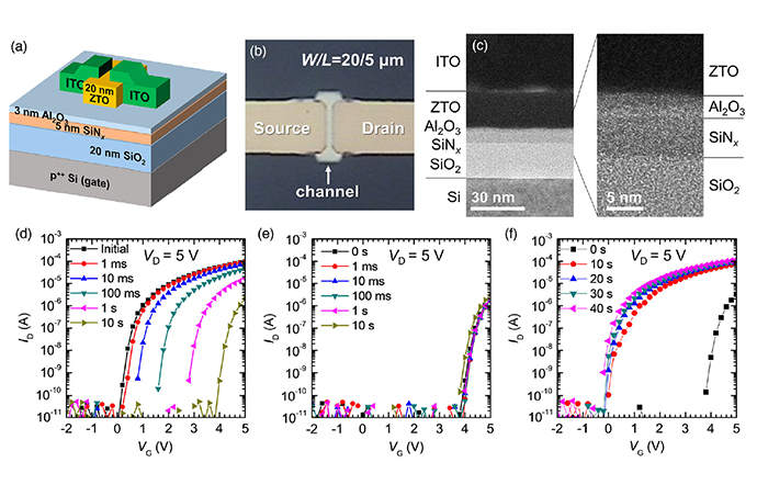
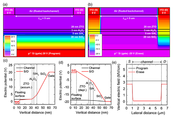
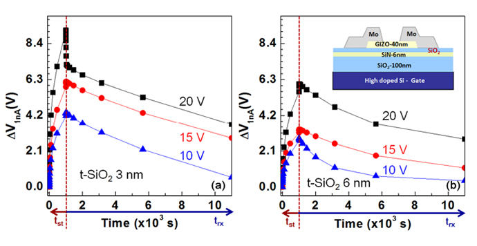
- A charge-trap flash (CTF) device is fabricated using atomic-layer-deposited zinc tin oxide (ZTO) as an n-type amorphous oxide semiconductor (AOS) channel layer and its program/erase characteristics are examined. A reasonable threshold voltage shift of 3.7 V was shown when a positive voltage of 20 V was applied to the gate electrode. However, even when -20 V is applied for up to 10 s, the trapped electrons are not detrapped. Instead, it is possible to recover Vth to its initial value only by irradiating white light. The high hole injection barrier between the source/drain and the ZTO channel prohibits hole injection, which is the cause of inefficient erasing. It is also confirmed that an AOS CTF with sufficient program and erase speed would be limited by the inherent energy band structure of AOS with its wide bandgap of over 3 eV.
Related Papers :
3. P-type SnO
3-1) Characteristics of SnO thin films with respect to Sn/O ratio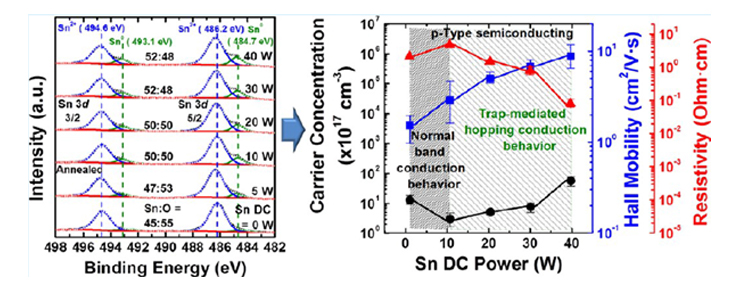
- The Sn/O ratio varied from 56:44 to 74:26 at the as-deposited state. After thermal annealing at 180 °C for 25 min under an air atmosphere using a microwave annealing system, the films were crystallized into tetragonal SnO when the Sn/O ratio increased from 44:56 to 57:43. Notably, the metallic Sn remained when the Sn/O ratio was higher than 55:45 at an annealed state. When the ratio was lower than 55:45 at the annealed state, the incorporated Sn fully oxidized to SnO, making the films useful p-type semiconductors. In contrast, the films became metallic conductors at higher Sn/O ratios. At the Sn/O ratio of 55:45 at the annealed state, the film showed the highest Hall mobility of 8.8 cm2 V-1s-1 and a hole concentration of 5.4 × 1018 cm-3. Interestingly, the electrical conduction behavior showed trap-mediated hopping when the Sn metal was co-sputtered, whereas the single SnO film showed regular band conduction behavior. The residual stress effect could interpret such property variation originated from the sputtering power and post-oxidation-induced volumetric effects.
Related Papers :
- S. J. Lee et al. "Composition, Microstructure, and Electrical Performance of Sputtered SnO Thin Films for p-Type Oxide Semiconductor." ACS Appl. Mater. Interfaces 2018, 10, 3810-3821
3-2) Electrical Instability of p-Type SnO Thin-Film Transistors
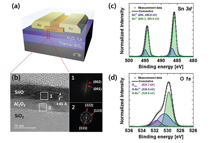
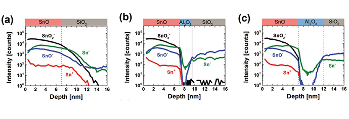
- Both experimental results and theoretical calculations show that the origin of border traps is the Sn+0 Si gap states in SiO2, induced by the Sn diffusion into the SiO2 layer. The use of Al2O3 films as ILs suppresses this diffusion. The Vhy of the SnO TFTs can be decreased when the thickness and density of the ILs are increased if the amorphous structure of the Al2O3 IL is maintained after the rapid thermal annealing process. P-Type ALD SnO TFTs with optimum ILs exhibit a high on-off ratio of IDS (1.2 × 10⁵), high field-effect mobility (1.6 cm2 V-1s-1), and a small Vhy (0.2 V).
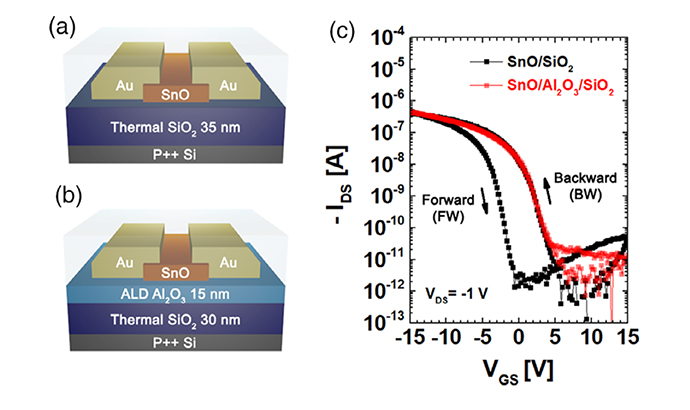
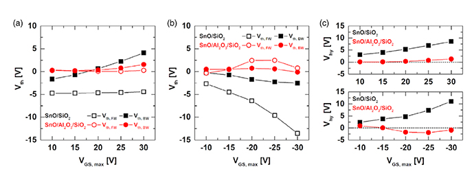
- The gate-induced electrical instability of SnO thin-film transistors (TFTs) with SiO2 and Al2O3/SiO2 gate dielectric layers is evaluated. The hysteresis voltage (Vhy) and threshold voltage (Vth) in the transfer characteristics of SnO TFTs depends on the sweep range and rate of gate voltage (VGS). The TFT with an Al2O3/SiO2 gate dielectric layer exhibit reduced Vhy and stable Vth compared with the device without an Al2O3 layer. The introduction of an Al2O3 layer between the SnO channel and the SiO2 layer suppresses the electron and hole trapping at the channel/dielectric interface and contains mobile oxygen vacancies that counteract the hole trapping effect.
Related Papers :
- Y. Jang, et al. "Reduction of the Hysteresis Voltage in Atomic-Layer-Deposited p-Type SnO Thin-Film Transistors by Adopting an Al2O3 Interfacial Layer." Adv. Electron. Mater. 2019, 1900371
- Y. Jang, et al. "Comparative Study on the Gate-Induced Electrical Instability of p-Type SnO Thin-Film Transistors with SiO2 and Al2O3/SiO2 Gate Dielectrics" Phys. Status Solidi RRL 2020, 2000304