 HOME > Research > Ferroelectric Devices
Ferroelectric Devices
(Hf, Zr)O2 ferroelectric materials & applications
Recently, it was reported that HfO2 can
show ferroelectric (FE) properties when doped with various dopants such as Zr,
Si, Y, Al, Gd, La, and Sr. Compared to the conventional ferroelectrics based on
perovskite or layered perovskite structure, such as Pb(Zr,Ti)O3 and
SrBi2Ta2O9, the FE HfO2-based films
showed quite distinctive physical and electrical properties. The HfO2-based
films can be extremely thin (film thickness, tf < 10 nm) with
feasible ferroelectricity (remnant polarization, Pr ~ 10–40 μC/cm2), whereas the much thicker thicknesses (tf >
100 nm) are required for the stable FE properties of conventional
ferroelectrics thin films, especially with the metal-ferroelectric-metal (MFM)
configuration. Due to their small thickness, the HfO2-based films
are considered promising for the three-dimensional capacitor structure which is
highly required for the future ferroelectric random-access-memory (FeRAM)
device according to International Technology Roadmap for Semiconductors. This
results from the relatively large bandgap (Eg ~ 5.5 eV), high compatibility
with Si, and matured atomic layer deposition (ALD) technique of HfO2-based
films. In fact, due to their high Si-compatibility, the non-FE HfO2
thin film has been used as the buffer layer in ferroelectric
field-effect-transistor (FeFET) to solve the interfacial problems of
conventional ferroelectrics and Si substrate.
HZO Thin film (polar phase & electrical properties)
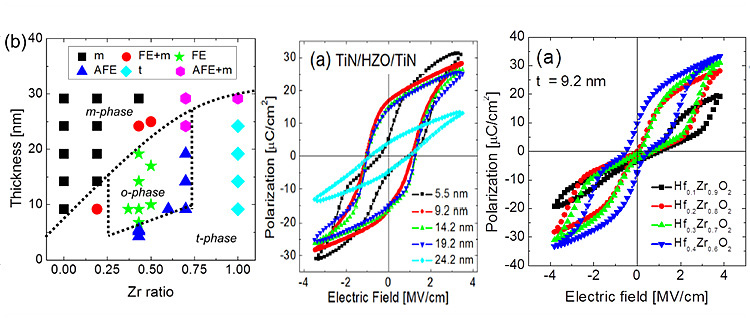
We examined the effect of tf on the FE properties
of the Hf0.5Zr0.5O2 films. They tested the Hf0.5Zr0.5O2
films with various tf (5.5–25 nm) and annealing temperature (400–800
°C). When the tf was ≈ 10 nm, the Pr
of the Hf0.5Zr0.5O2 films was the largest (≈ 15 μC cm−2), whereas the Pr decreased to ≈ 12 and ≈ 5 μC cm−2 when the tf
increased to 17 and 25 nm, respectively. This could be understood from the fact
that the portion of the m-phase increased as the tf increased.
Meanwhile, we also found that the insertion of thin (~1nm) dielectric Al2O3
inter-layer between 20-nm- thick Hf0.5Zr0.5O2
layers can prevent the continuous growth of the whole Hf0.5Zr0.5O2
films, and the FE properties was not degraded with increasing tf.
The origin of the formation of an unexpected FE phase was
systematically examined for Hf0.5Zr0.5O2 films
by our group. Since the growing nuclei are supposed to have t-phase structure
prior to the zipping, and because of the surface energy effect, there must be
several variations in the resulting strain states after the zipping, according
to the original crystallographic directions of the nuclei. Using the in-plane
stress condition of the film, we could calculate the strain along the a-, b-,
and c-axis of the grains of various orientations using the in-plane stress
conditions of the thin film. As a result, the 110- orientation was the most
favorable for the formation of the o-phase from t-phase, whereas the 111-
orientation was the worst, since almost equivalent strains were formed along
the a-, b-, and c-axis (none of the a-, b-, and c-directions can be tensile
while other direction is compressive).
Related Paper:
M. H. Park, et al., Advanced Materials, 11,
27, 1811-1831 (2015)
M. H. Park, et al., Appl. Phys. Lett. 104, 072901 (2014)
H. J. Kim, et al., Appl. Phys. Lett. 105, 192903 (2014)
M. H. Park, et al., Appl. Phys. Lett. 105, 072902 (2014)
M. H. Park, et al., Appl. Phys. Lett. 102, 242905 (2013)
Wake Up Effect of HZO Thin Film
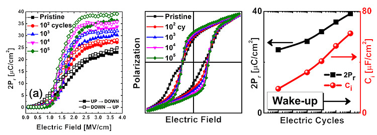
The Hf0.5Zr0.5O2 film shows
mostly ferroelectric (FE)-like behavior in the pristine state, where the slight
anti-ferroelectric (AFE)-like distortion could be ascribed to the anti-parallel
distribution of some of the FE domains and the AFE phase. The field cycling of
only 100 cycles almost completely removed such anti-parallel pinned domains.
Further increase in the field cycling number more effectively poled the domains
making the Pr increase significantly. Field cycling also transformed
the non-FE phases, mostly at the electrode interface, to the FE-phase, which
could be inferred from the increase in the interfacial capacitance. These
results indicate that the physical state of the FE-phases in the HZO film is
quite different from the conventional FE thin films, such as PZT, in a sense
that it is the outcome of variously oriented domains, possibly including
anti-parallel orientation. Field cycling plays a role in poling in conventional
FE materials, but the high field-induced non-FE t-phase to FE o-phase
transition could also contribute to the effective poling (depinning of the
pinned FE domains).
Related Paper:
H. J. Kim, et al., Nanoscale, 8, 1383-1389 (2016)
Two-Step Polarization Switching Mediated by a Nonpolar Phase in HZO Thin Film
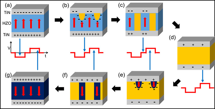
The broken hysteresis loop in the P–E test and two-step
polarization switching in pulse switching measure measurement from Hf0.4Zr0.6O2
films were systematically examined based on the first-order-like phase
transition theory. The broken hysteresis behavior Hf0.4Zr0.6O2
film could be understood based on the classical theory on the first order phase
transition, where the NP phase is involved during the transition from one
polarization state to the opposite polarization state. The expected two-step
(UP → NP (region I) and NP → DOWN (region II)) polarization switching could be
also confirmed by dynamic pulse switching measurement.
Related Paper:
M. H. Park, and H. J. Kim, et al., Nanoscale,
DOI:10.1039/c5nr08346j (2016)
Monolithic Device with Various Devives for Pyroelectric Energy Harvestor/Electro Caloric Device, High-Charge Capacitor/Electrostatic Energy Storage, and IR Sensing.
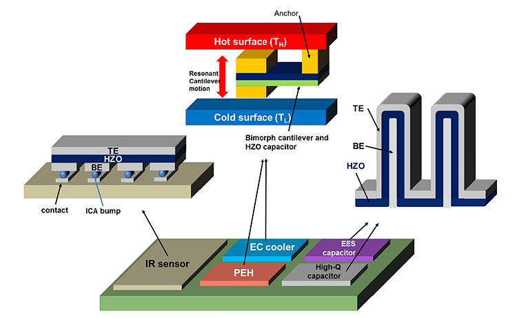
The schematic images of the HZO-based monolithic device for
pyroelectric energy harvesting (PEH), electrocaloric effect (ECE),
electrostatic energy storage (EES), a high-charge capacitor, and infrared (IR)
sensing fabricated on Si substrates. The upper center panel shows the
schematics of a PEH device based on microelectromechanical systems, which was
designed by Oak Ridge National Laboratory. A cantilever is positioned between a
hot surface and a cold surface, and the resonant motion of the cantilever can
be produced due to the difference in the thermal expansion coefficient of the materials in the bimorph part.
Furthermore, the appropriate combination of the cycling of the electrical field with the resonant motion can use the PEH or the
ECE. The PEH and the ECE are inverse cycles, so they can be easily used in an
equivalent structure merely by changing the sequence of the applying field and changing T. The upper right panel shows the
structure of an EES or a high-charge capacitor, which are based on a simple
capacitor structure with top and bottom electrodes. For HZO, TiN might be the
best electrode material, and the three-dimensional capacitor structure was used
to increase the ESD and the stored charge by increasing the area of the
capacitor. With the appropriate external circuit, the EES capacitors with an
HZO dielectric layer can store the energy harvested by a PEH device using
another HZO film. The upper left panel shows the schematics of an array-based
pyroelectric IR detector. It is believed that the Si compatibility of HZO films
might make the IR detector more appropriate for mass production. These
functional devices could be produced on Si wafers and could be stacked with the
Si processors or memory chips that are the sources of the waste heat, or placed
near the chips on the printed circuit board.
Related Paper:
M. H. Park, et al., Nano Energy, 12, 131-140
(2015)
Electrostatic Supercapacitors with Large Energy Storage Density
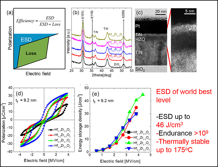
The energy storage characteristics of a new lead-free AFE HfxZr1-xO2 (0.1 < x < 0.4) materials system were examined. The thin HZO capacitors could have an ESD higher than ≈ 30 J cm−3 in the wide x-value range of 0.1–0.4, which is a crucial advantage for their mass production. The ESD of the 9.2-nm-thick Hf0.3Zr0.7O2 capacitor was the largest among the HZO films with various compositions, and the maximum ESD was 46 J cm−3 at the 4.5 MV cm−1 electric field. The ESD of the Hf0.3Zr0.7O2 capacitor decreased with an increase in the film’s thickness, likely due to the increased formation of the m-phase, but was still as high as ≈ 21 J cm−3 when tf was 29.0 nm. The ESD and energy efficiency of the Hf0.3Zr0.7O2 capacitor did not decrease with the increase in the temperature up to 175 °C, which shows its robust thermal stability that makes it appropriate for practical application. Moreover, the large ESD decreased by only ≈ 4.5% even after 109 times of field cycling at a switching electric field of 3.26 MV cm−1 . All the dielectric films were deposited using the ALD method at a substrate temperature of 280 °C, which demonstrates the compatibility of the material and the process with nanostructured devices.
Related Paper:
M. H. Park, et al., Advanced Energy Materials, 16, 4,
1400610 (2014)
Ferroelectric/Dielectric Bilayer electronic devices - Theoretical work on ferroelectric/dielectric bilayer structure
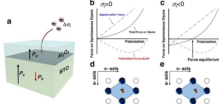
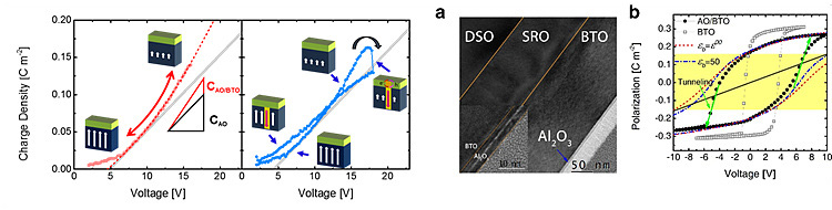
Enhancement of capacitance by negative capacitance (NC)
effect in a dielectric/ferroelectric (DE/FE) stacked film is gaining a greater
interest as a feasible solution to miniaturize capacitors and field effect
transistors for future semiconductor devices. Since its model was first
suggested, several experimental proofs on the capacitance boost of DE/FE
stacked films were reported. However, the previously reported theoretical
background of this intriguing effect holds a self-contradictory problem.
Therefore, this work suggests an alternative model to describe the negative
capacitance effect in a DE/FE system quantitatively. This work adopted a
modified formalism to incorporate the depolarization effect to describe the
energy of the general DE/FE system. The model predicted that the SrTiO3/BaTiO3
system will show a capacitance boost effect. It was also predicted that the Al2O3/BaTiO3
(AO/BTO) system shows the capacitance boost effect with no FE-like hysteresis
behavior. However, the involvement of the trapped charges at the DE/FE
interface, originating from the very high field across the thin Al2O3
layer when the BTO layer played a role as the NC layer, can frustrate, the NC
effect in the AO/BTO system. Under this circumstance, the highly stored charge
by the NC effect of the BaTiO3 during the charging period could not
be retrieved during the discharging process because integral part of the polarization
charge was retained within the system as a remnant polarization.
Related Paper:
Y. J. Kim, et al., Scientific Reports, 6, 19039 (2016)
Tunnel Switch Device
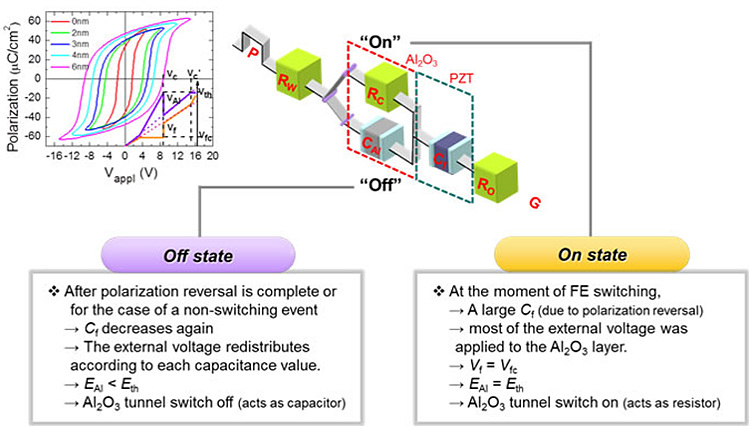
Ferroelectric random access memory devices (FeRAM) have
attracted a great deal of interest as a potential replacement for non-volatile stand-alone
memory devices or as a memory element in a system-on-chip device where a high
density (> 16 mega bit) is preferred for the device performance and cost
effectiveness. However, scaling down the ferroelectric thin films has some
practical problems. One of them is that Interfacial effects become increasingly
severe as the ferroelectric layer thickness decreases, which has made
ultra-thin ferroelectric film applications virtually impractical. On the
contrary, an interfacial layer can be used positively. It is possible that this
interfacial layer (tunnel switch layer) can be utilized constructively to
improve the reliability of a FE capacitor if by-electrode charge injection is
blocked by this layer. Of course, this layer should not interfere with polarization
switching.
Related Paper:
A. Q. Jiang, et al., Advanced Materials,
21, 2870-2875 (2009)
Tri-state Memory
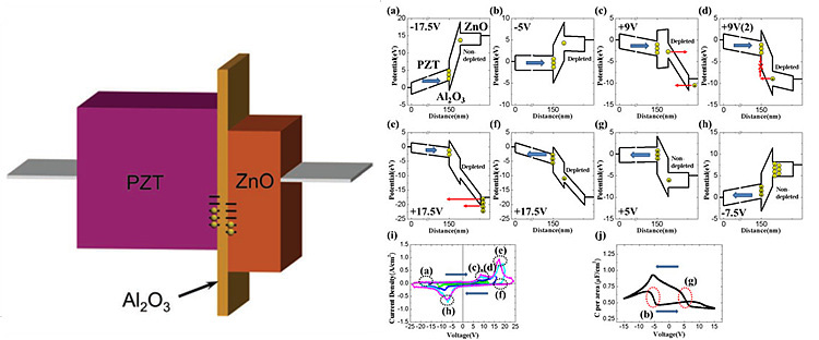
Ferroelectric memory has been one of the most attractive
candidates for the next generation nonvolatile memory application. However,
conventional researches on FeRAM(Ferroelectric Random Access Memory) is
decreasing gradually due to its intrinsic problems, such as large size of unit
cell(14~25 F2). Thus, there has been much efforts to reduce the cell
size of the FeRAM. However, there were not so impressive advances in this
field, and some innovative idea is needed to meet the requirement of the
reduced sized FeRAM.
If reducing the cell size is impossible, writing more
than two states could be a new solution for the problem of scaling. In this
study, 3-states memory was fabricated and its mechanism was studied using
PZT/Al2O3/ZnO trilayer. Even though, a unit cell of
3-states memory cannot be the multi-bit memory by itself, two unit cells of
3-states memory can substitute the three unit cells of 2-states memory. Thus,
it is possible to memorize the 50% increased data with the help of peripheral
circuit.
Related Paper:
M. H. Park, et al., Advanced Functional Materials, 22,
21, 4305-4313 (2011)