 HOME > Research > Logic and In-memory Computing
Logic and In-memory Computing
Logic and in-memory computing
- In-memory computing, whose computation is performed within a nonvolatile memory array without data movement, has attracted attention these days due to its energy/power efficiency, high throughput, and wide range of applications. The memristive logic gates can implement all basic logic functions, which can be expanded for the memristive arithmetic logic unit. In addition, the gradual conductance property can be utilized in the analog computing field, which is commonly used in deep learning and neuromorphic application.
1. Logic-in-memory: stateful and sequential logic using nonvolatile memory
- Modern computing systems are based on von Neumann architecture in which the processor and memory are separated physically. The emerging data-centric applications and the memory wall problem necessitate a new computing architecture. The technology called logic-in-memory (LIM) utilizes nonvolatile memory eliminating data migration between memory and computing unit, which enhances the computation speed and lowers the energy consumption. Utilizing the small cell size (4F2) of a nonvolatile resistive switching random-access memory (RRAM) and the inherent characteristic of the gradual conductance change, digital and analog LIM can be realized.
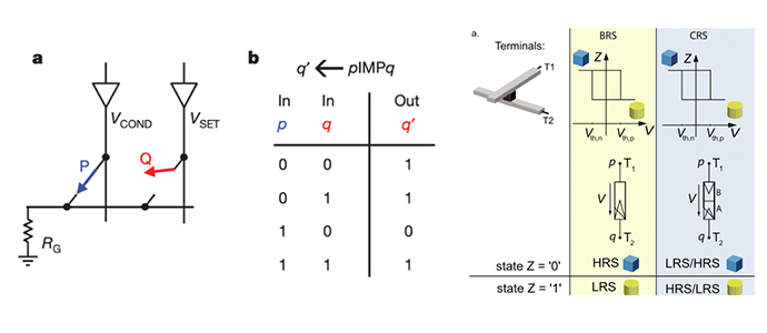
- The representative work on the stateful memristive logic, also called R-R logic, was proposed by J. Borghetti named IMPLY-logic in 2010. The primitive circuit is comprised of two parallel memristors P and Q connected to a series resistor, as shown in Figure 1-1(a). The material implication function can be achieved by performing a conditional operation by applying two applied biases, Vcond and Vset. Since the input and output are represented by the resistance of a memristor, the IMPLY-based basic function, as shown in Figure 1-1(b), can be cascaded to any other compound Boolean logic. Thus, all sixteen distinct binary Boolean operations can be demonstrated on two logic values with the combination of IMP and FALSE functions.
- The other logic family is sequential memristive logic, or V-R logic, which uses voltage-type input and resistance-type output, as represented in Figure 1-1(c). Based on the I-V behavior of the BRS and CRS memristor device, a finite state machine (FSM) can be constructed with resistive state variables and conditional variables of the nodal voltage. Linn's BRS and CRS logic demonstrates 14/16 Boolean logic operations within three sequential cycles. The discrepancy of the voltage-type and resistance-type limits the cascading of the two missing Boolean logic operations. Later, the complete binary logic function was implemented by You et al. using BiFeO3 bilayer structure for compact sequential logic.
2. New logic primitive circuit and standardization
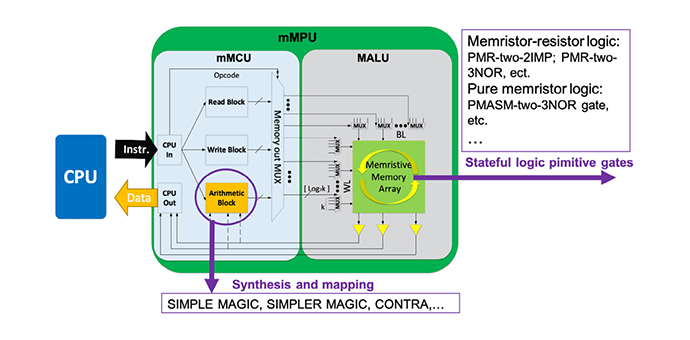
- So far, many branches of the two logic families have been proposed, such as IMPLY, TSML, MAGIC, and MRL, to increase the functionality of the basic logic functions. Our group standardizes the nomenclature of the primitive circuit by "structure of the primitive logic gate" - "number of logic inputs" - "n (implemented basic logic function)," for the better comprehensive understanding and improvement from the survey, where n represents the number of memristors used in the logic gate.
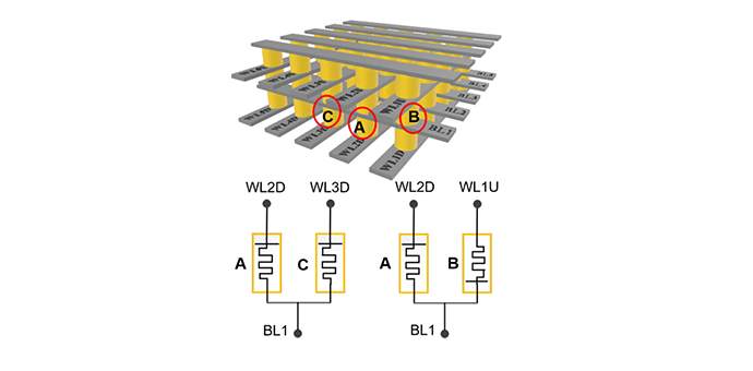
- The new primitive logic gate based on the two antiparallel bipolar resistive switching (BRS) memristors with a series resistor is proposed in our group named APMR-two-(IMP,AND,TF) gate that can be configured in the 3D crossbar array (CBA) structure. This new implementation allows the capability of the other primitive logic gates such as PMR-two-2IMP, PMASM-two-3NOR, and PMR-two-3NAND. The six basic operations of IMP_q, IMP_p, AND_p, AND_q, FT_pq, and TF_pq can be implemented in a single cycle. Then, the six basic operations can be effectively used to demonstrate complete logic functionalities. The scope of the research includes logic device tuning with line resistance and local electrode engineering, designing system architecture, and improvement in reliability and LIM efficiency.
Related Papers :
- N. Xu, T. Park, et al. "A Stateful Logic Family Based on a New Logic Primitive Circuit Composed of Two Antiparallel Bipolar Memristors." Adv. Intell. Sys., 190082 (2019).
- N. Xu, T. Park, et al. "In-Memory Stateful Logic Computing Using Memristors: Gate, Calculation, and Application." Phys. Status Solidi RRL, 2100208 (2021).
- T. Park et al. "Reliable Domain-Specific Exclusive Logic Gates Using Reconfigurable Sequential Logic Based on Antiparallel Bipolar Memristors." Advanced Intelligent Systems, 2100267 (2022).
Related research group homepage
- FuST Research. - Future Semiconductor Technology laboratory (kaist.ac.kr) - Prof. Kyung Min Kim
3. Towards arithmetic logic unit with memristive logic circuit
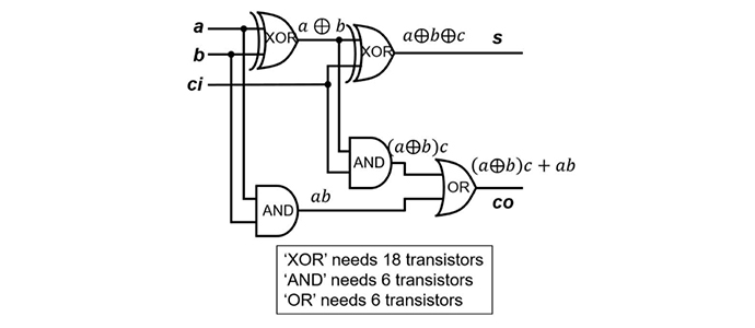
- Arithmetic logic unit (ALU), the fundamental combinational circuit for binary bitwise operations, is the basis for the multiple applications involved in computations. Among the ALU operations, full adder (FA), which operates bitwise addition, is a fundamental and essential building block since other operations such as multiplication, division, and subtraction can be derived. A CMOS-based computation system implements the FA with transistors. For example, a CMOS-based 1-bit FA, composed of one OR gate (6 Trs), two AND gates (2x6 = 12 Trs), and two XOR gates (2x18 = 36 Trs), requires 54 transistors, as shown in Figure 3-1. Although replacing with NAND gates can further reduce the number of transistors, a way to further reduce the area cost for ALU is essential for the higher density to increase the overall performance.
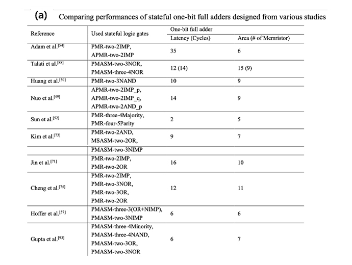
- For a decade, the LIM community has focused on implementing memristive logic gates that can complete logic functionalities. At present, the efficiency to implement memristive 1-bit FAs is prioritized, and many memristive FAs are reported, as represented in Figure 3-2(a). It shows that latency and area costs are tradeoff relationships and demonstrates the efficiency in terms of area cost compared to the CMOS-based implementation.
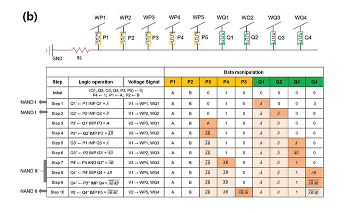
- The proposed APMR-two-(IMP,AND,TF) gate can implement 1-bit FA on 9 memristors with 14 sequential cycles, as shown in Figure 3-2(b). Compared to CMOS-based FA, the proposed 1-bit memristive FA can reduce area cost from 324F2 to 36F2.
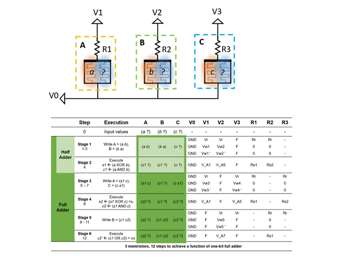
- Another stateful logic gate, the time-efficient stateful dual-bit memristor (DBM) logic, composed of single URS-BRS dual bit memristors with a series resistor, is also proposed in our group. The dual bit stateful logic gate can implement 1-bit FA on 3 memristors with 12 sequential cycles, using multi-functionalities in a single memristor, as shown in Figure 3-3, which reduces area cost to 12F2.
- Although the reduction of the area cost in stateful logic reveals worthwhile, the latency still has to be addressed to give a meaning of "practical." The community is now shifting toward the n-bit input expansion. Most memristive adders are based on the ripple-carry method, which has a high time cost in carry propagation. The memristive carry-look-ahead, carry-save, and parallel prefix adder are being researched to address the propagation delay.
- Our group focuses on an efficient way to improve the memristive ALU system and possible limitations regarding practical applications in the array-level implementation. The array-compatible memristive logic and device modeling are under development to interconnect simulation and hard-level implementation.
Related Papers :
- N. Xu, L. Fang et al. "Time-Efficient Stateful Dual-Bit-Memristor Logic." Phys. Status Solidi RRL, 1900033 (2019).
4. In-memory computing using analog memristors
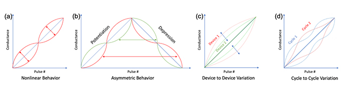
- Analog memristor, whose gradual conductance changes within a controllable manner, is a candidate to further expand memristive applications beyond the digital applications, such as the content addressable memory (CAM) and physical unclonable function (PUF) shown in Figure 4-1(a) and (b), respectively. The digital computing is useful in the fields such as the "right or wrong" problem, but various fields of the emerging application are involved in an analog manner, especially in energy/power saving, the precise calculation for numerical analysis, and real-time/space signal processing.
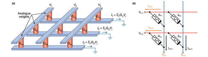
- One of the analog applications is vector-matrix multiplication (VMM), which is the main operation in neural network (NN) since each cell in Figure 4-3(a) can be the physical counterpart of NN's neuron-synapse connection. Using Kirchhoff's and Ohm's law, the VMM can be implemented on memristive CBA by applying the voltage and collecting the current through peripheral circuits, as shown in Figure 4-3(b). Compared to the CMOS-based ALU units or SERDES, a highly parallel and pipelined calculation can be achieved without having complexity.
Related Papers :
- Yumin Kim et al. "Kernel Application of the Stacked Crossbar Array Composed of Self-Rectifying Resistive Switching Memory for Convolutional Neural Networks." Adv. Intell. Syst. 1900116 (2020).
- Jihun Kim et al. "In-Depth Analysis of One Selector-One Resistor Crossbar Array for Its Writing and Reading Operations for Hardware Neural Network with Finite Wire Resistance." Adv. Intell. Syst. 2100174 (2021).
- Yu Yan et al. "Area-Type Electronic Bipolar Switching Al/TiO1.7/TiO2/Al Memory with Linear Potentiation and Depression Characteristics." ACS Appl. Mater. Interfaces 13, 39561-39572 (2021).