 HOME > Research > Resistive Switching RAM
Resistive Switching RAM
Resistive Switching mechanism study
Resistive switching (RS) memory is a strong
contender for highly scaled next generation non-volatile memory devices. It has
been well known that the RS behaviors mainly rely on the controllable soft
breakdown in normally insulating films through the electroforming process of
conducting nano-channels so-called filaments and their repetitive rupture and
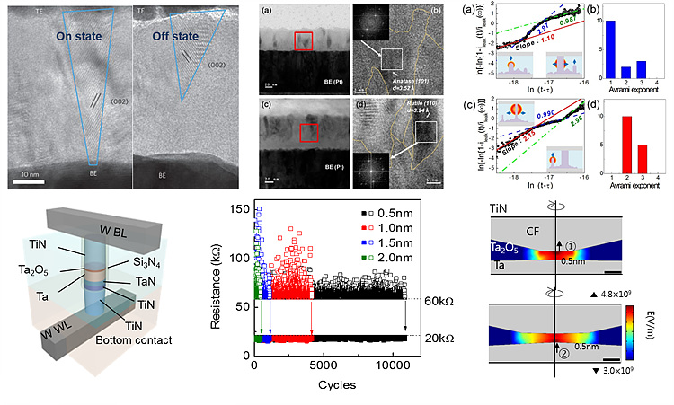
rejuvenation process. It was verified that the Magnèli phase (TinO2n-1,
n≥4) transition plays a crucial role in the RS operation mechanism in TiO2
based RS memories through extensive high-resolution transmission electron
microscopy and electron diffraction analyses. It was the very first time that
conductive filaments were observed directly. Further electronic or ionic
bipolar resistive switching characteristic occurring at the filament ruptured
region was studied.
An
additional method that identify the real-time evolution of conducting
nano-filament by applying the Johnson-Mehl-Avrami type kinetic model is
conducted. In PEALD sample whose pristine state is anatase phase, the
rejuvenation of the filament is accomplished by repeated one-dimensional
nucleation followed by a two-dimensional growth. In sputtered film whose
pristine state is rutile phase, however, one-dimensional nucleation-free
mechanism dominates because of compatibility between rutile and Magnèli phase.
On
the other hand, Ta2O5 based RS memories show different
switching behavior because they have no stable and oxygen-deficient phase in
Ta-O systems. In this systems, filaments are formed by the drift of oxygen
vacancies under the application of electric field. It is hard to exquisitely
control the RS behavior in ultra-thin and small devices because the shape of
the conductive filament looks like an hour-glass. As such, the formation and
rupture of the filament should be conducted by the same polarity voltage.
Related Papers:
K. M. Kim, et al., Appl. Phys. Lett. 90 24,
242906 (2007)
K. M. Kim, et al., Appl. Phys. Lett. 91 1,
012907 (2007)
K. M. Kim, et al., Appl. Phys. Lett. 94 12,
122109 (2009)
D. H. Kwon, et al., Nature Nanotechnol. 5,
148-153 (2010)
S. J. Song, et al., Appl. Phys. Lett. 96 11,
112904 (2010)
K. M. Kim, et al., Nanotechnology 21 30,
305203 (2010)
K. M. Kim, et al., Nanotechnology 22 25,
254010 (2011)
K. J. Yoon et al., Nanotechnology, 18, 23,
185202 (2012)
S. J. Song, et al., Sci. rep. 3, 3443 (2013)
K. J. Yoon et al., Nanotechnology, 14, 24, 145201 (2013)
K. J. Yoon et al., Nanoscale, 6, 2161
(2013)
Improving the Resistive Switching Property
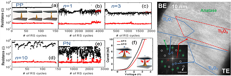
Improved electrical endurance can be
obtained in a crossbar type Pt/TiO2/Pt structure by using a modified
bias scheme. With a conventional bias scheme, for example positive set and
positive reset, conical shape conduction filament having a narrower cross
sectional area at the anode interface is formed in the TiO2 memory
layer. Because resistive switching occurs near the top electrode, it causes a
rapid oxygen consumption leading to the poor electrical endurance. To prevent
the rapid oxygen consumption, a modified bias scheme composed of a series
application of positive and negative bias is used. As a conical filament shape
is generated by a single bias scheme, the modified bias scheme results in an
hourglass shaped conduction filament as confirmed by the HRTEM of the device
after repeated switching cycles. Eventually, the oxygen consumption is
effectively suppressed and the switching endurance was highly improved.
Related Papers:
K.M. Kim et al., Electrochemical and
Solid-State Letters, 6, 13, G51-G53 (2010)
G. H. Kim, et al., Appl. Phys. Lett. 98, 262901 (2011)
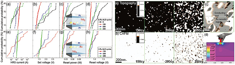
Switching uniformity is another critical issue
for resistive switching memory. The formation and rupture of conduction
filament are stochastic phenomena so they give highly scattered operation
parameters. The variability of the operation parameters was compared for the
cases where Ru nano-dots were embedded in the vicinity of bottom or top
interface region of a Pt/TiO2/Pt resistive switching cell. Combined
with ATLAS simulation results, the AFM and CAFM analysis reveal that the Ru
nano-dots role as either a local field enhancer or field suppressor when
inserted at the cathode or anode interface, respectively. Therefore, limiting
the location where electron injection occurs at the cathode interface to a
narrower region was the key factor for achieving highly improved RS uniformity.
Related Papers:
J. H. Yoon, et al., Appl. Phys. Lett. 97,
232904 (2010)
J. H. Yoon, et al., Adv. Mater. 25, 1987-1992 (2013)
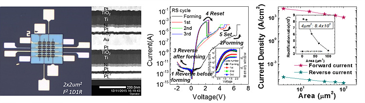
Selector Employed 3D RRAM Crossbar Array Intergration
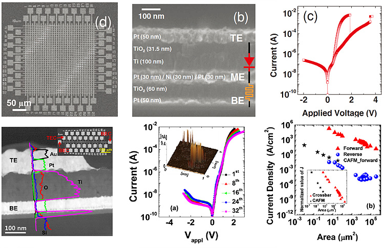
32x32 crossbar array(CBA) of >1kb RRAM
was fabricated. Each cell is comprised of 1diode-1resistive switching memory
stack, where a diode selector was employed for each resistive switching element
to alleviate the sneak currents issue in the CBA. In order to accomplish the
stack, a Pt/TiO2/Ti/Pt diode was stacked above a Pt/TiO2/Pt
unipolar resistive switching memory. The diode selector adopted the TiO2
deposited by ALD method with O3 as the oxidant. The maximum
rectification ratio achieved in the diode was >106, while it was
>105 in the 1D1R device. The high rectification ratio is
attributed to the high Schottky barrier at the Pt/TiO2 and the
quasi-Ohmic conduction through the TiO2-x/Pt, which is obtained by
the partial oxidation of Ti during the subsequent oxide deposition. Conduction
through a local conducting paths was confirmed for the both injections, based
on the electrode area dependent current density and the conducting AFM
measurements.
Related Papers:
G. H. Kim et al., Adv. Funct. Mater., 11,
23, 1440 (2012)
G. H. Kim et al., Appl. Phys. Lett. 21, 100, 213508 (2012)
Double-layers stacked RRAM was demonstrated in 4x4x2 CBA. In order to avoid the thermal disruption issue during the stacking process, which is particularly critical for the diode layer embedding high chemical potential within the layer, room temperature sputtering was adopted for the deposition of every oxide layer. The room temperature fabricated Pt/TiO2/Ti diode showed even improved property with the rectification ratio of >108, which was still maintained in the 1D1R device. The enhancement in the diode rectifying property is mainly ascribed to the suppression of the partial reduction of TiO2, which degrades the performance of Schottky barrier at the Pt/TiO2 interface. A 2-bit operation of the 1D1R further scaled the cell size down to F2.
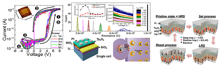
Due to the low per lithographic margin of
the aforementioned stacked RRAM structure, vertical RRAM structure adopting
etching process as the key fabrication technique is preferred. Since the middle
electrode placed in between the selector and the memory can no longer be
adopted in this structure, however, a self-rectifying RRAM comprised of only
the two different oxide layers is developed. The Pt/Ta2O5/HfO2/Ti
device showed a resistive switching based on trapping/detrapping mechanism,
accompanied with high rectification ratio of ~106. Furthermore,
the highly promising 3-bit operation was demonstrated.
Related Papers:
J. H. Yoon et al.,
Adv. Funct. Mater., 32, 24, 5086 (2014)
J. H. Yoon et al., Adv. Mater., 25, 27, 3811 (2015)
Study on Crossbar Array Architecture
The diode requirements based on the sneak
currents analysis in a planar CBA has been examined. In CBA structure, the
sneak current paths comprise a parallel resistor component to a selected cell.
Therefore, unwanted sneak currents can interrupt the accurate reading of the selected
cell. By calculating all the possible sneak current components within a CBA,
the required rectification ratio and the forward current density of the diode
according to memory density has been evaluated.
Related Papers :
G. H. Kim et al., Nanotechnology, 21, 385202
(2010)
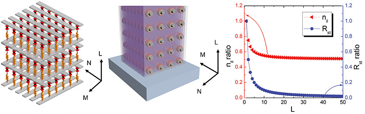
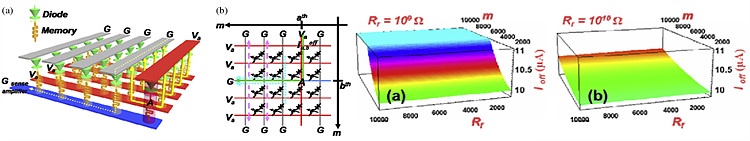
Further improved from the sneak currents
analysis in the planar CBA, sneak currents analysis on 3dimensional- (3D-) CBA
was examined. Two ideas of realizing the 3D RRAM structure was proposed:
cross-line structure, and word-plane structure. The cross-line CBA is the
structure where multiple layers of planar CBA are repetitively stacked, whereas
the word-plane structure is the structure where the selector and memory oxides
are overlaid on a vertically erected metal sidewall structure. Particularly for
the latter, the number of bit-lines sharing a word-line increases with the
increasing number of layers, therefore, sneak currents problem gets severer
with the increasing number of layers. Therefore, higher selector performance is
required for the word-plane structure compared to that of the cross-line
structure. However, the high per lithographic margin of the word-plane makes
the structure highly cost-effective, which is favorable for the ultimate
success of the 3D RRAM.
Related Papers :
J.Y. Seok et al., Adv. Funct. Mater., 34,
24, 5316-5339 (2014)
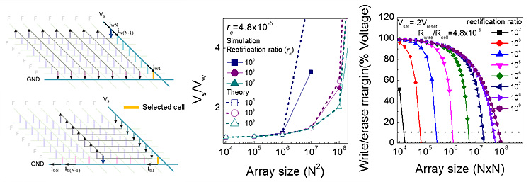
On the other hand, it has been recently found that the sneak currents can be problematic even during writing operation. The sneak currents may incur adverse voltage drop on the selected word- and bit- line and may also disturb the unselected cells on the sneak current paths. An analytical model for evaluating the increased writing voltage as well as the decreased writing margin due to the additional voltage drop on the selected word- and bit- line by the involvement of sneak currents has been deduced. A HSPICE simulation results provide the validity of the analytical model, while the model was applied to the 1D1R device eventually providing a plausible design strategy of the device in order for its implementation to a high density CBA RRAM.
Neuromorphic Engineering
Introduction to Neuromorphic Engineering
Neuromorphic engineering means the concept describing the use of very-large-scale integration (VLSI) systems containing electronic analogue circuits to mimic neuro-biological architectures present in the nervous system. The implementation of neuromorphic computing on the hardware level can be realized by oxide-based memristors, threshold switches and transistors.
Relaxation oscillator-based leaky integrate-and-fire
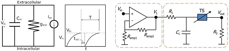
Leaky integrate-and-fire (LIF) model is the
most popular model of a neuron. Leaky integrate-and-fire model consists of a
capacitor like cell wall in real neurons and a resistance to make a leakage
current. (Left figure) As input current is applied, voltage difference between
extracellular and intracellular is increased. When the voltage reaches to
threshold voltage, LIF neuron fires a spike and the voltage comes back to
resting voltage.
One way to construct hardware LIF neuron is using relaxation oscillator as LIF neuron, so called relaxation oscillator-based LIF neuron (ROLIF neuron). The right figure shows structure of ROLIF neuron which uses Pearson-Anson oscillator (PAO) as relaxation oscillator. As input current is applied, voltage on threshold increased because of the capacitor. When the voltage reaches to threshold voltage, threshold switch (TS) is changed to low-resistance state (LRS) and it causes increase of Vout which means spike firing. Since TS is changed to LRS, voltage on TS becomes lower and it makes TS changed to high-resistance state again.
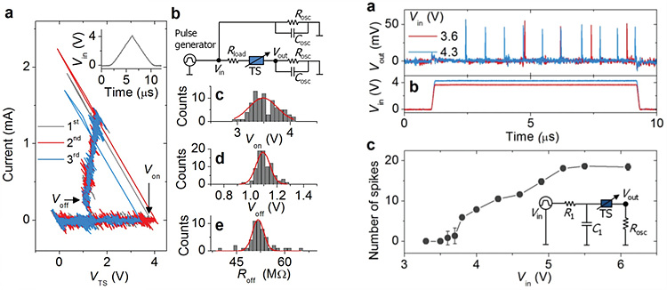
In ROLIF neuron, properties of threshold
switch are very important. For example, the left graphs shows the properties of
Pt/GeSe/Pt TS.
Top-right graph shows the spike train from
ROLIF neuron. The activity, the number of spikes in a given time period(8 μs), tends to increase with Vin.
To highlight this relationship, we further
identified the change in the number of spikes upon Vin (right-bottom
graph). First, the graph reveals that there exists a threshold voltage for
spiking (ca. 3.5 V) that is determined by Von. At Vin
below this threshold, VTS cannot reach Von, so no spike
is evoked. Second, the number of spikes tends to gradually increase with
increasing Vin in a wide Vin range. This change in the spike number
is attributed to a decline in the inter-spike interval (ISI) with Vin.
Third, the activity is saturated at a high Vin (>ca. 5.2 V). The
capacitor’s charging and discharging is in need of
non-vanishing time. Thus, this minimally required time delimits the minimum
ISI, i.e., maximum spike number.
Related Paper:
H. Lim et al., Nanoscale, 18, 9629-9640 (2016)