 HOME > Research > DRAM Capacitor
DRAM Capacitor
DRAM capacitor research
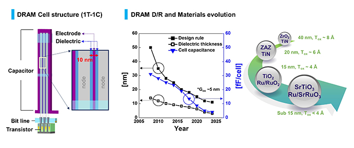
- The DRAM capacitor was changed to a metal-insulator-metal (MIM) structure to remove interfacial layers with low dielectric constant at the interface between polysilicon and dielectric material in SIS or MIS capacitors.
- Due to the extreme limitation on physical size (design rule of sub 15 nm) of capacitors in DRAM, a three-dimensional structure such as trench hole/stack type is required for Gbit-scale DRAMs to obtain sufficient storage capacitance. Therefore, atomic layer deposition and chemical vapor deposition (ALD and CVD) techniques providing excellent conformality are required to fabricate the top and bottom electrodes as well as the dielectric films.
- 1) Seo et al. Advanced Electronic Materials (2022).
- 2) An et al. Physica status solidi (RRL)- Rapid Research Letters 13, 1800454 (2019).
- 3) Hyun et al. Advanced Electronic Materials 6, 1-10 (2020).
- 4) Cha et al. Physica status solidi (RRL)- Rapid Research Letters 13, 1900282 (2019).
- 5) Kim et al. Advanced Materials 20, 1429-1435 (2008).
- 6) Unpublished (유전박막연구실).
- 7) Jeon et al. ACS Applied Materials and Interfaces 6, 21632-21637 (2014).
- 8) Lee et al. Chemistry of Materials 25, 953-961 (2013).
- 9) Lee et al. Chemistry of Materials 27, 3881-3891 (2015).
- 10) Kim et al. Physica status solidi (RRL)- Rapid Research Letters 13, 1900373 (2019).
1. Ru and RuO2 electrode films
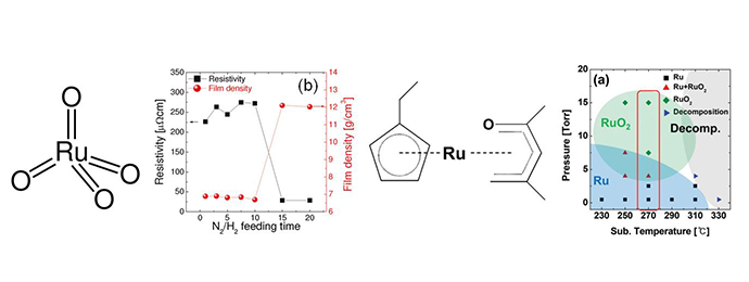
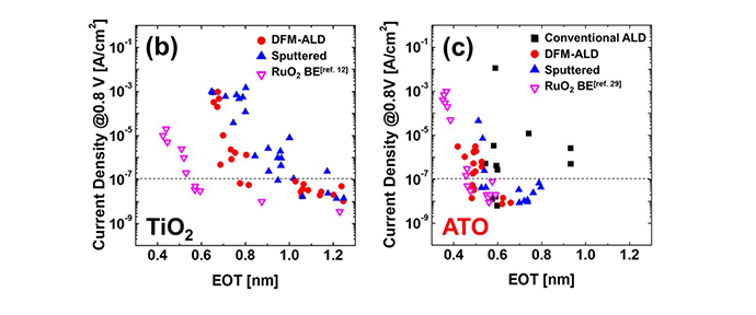
1-1) ALD/CVD processes for the Ru-based thin films- Ruthenium (Ru) is one of the most attractive materials for the DRAM electrode due to its promising properties, such as low resistivity (7.1 μΩ·cm) and high work function (4.7 eV). Even when Ru metal is oxidized to RuO2, it still maintains high electrical conductivity (resistivity: ~46μΩ·cm) and displays higher work function (5.1eV), making it suitable for DRAM applications. Numerous Ru precursors, such as RuO4 and Ru(EtCp)(DMOPD), have been investigated for Ru-based electrode materials.
- Ruthenium tetroxide (RuO4) precursor has a very simple structure with a small molecular size, making it adaptable for deposition of Ru or RuO2 electrode films on a complex structure. The phase of electrode films could be controlled by the injection time of H2-reduction gas, RuO2 for a shorter H2 injection time, and Ru for a longer time. RuO2 films deposited by thermal decomposition of RuO4 precursor were reduced to intermediate states (RuOx, 0
- Ru(EtCp)(DMOPD) [(2,4-dimethyloxopentadienyl)(ethylcyclopentadienyl)Ru] precursor was used for the ALD-Ru process with O2 as a reactant gas. The ALD growth behavior of the Ru films could be observed on various substrates. The higher growth per cycle (GPC) of 0.83 Å/cy was obtained with stable growth behavior compared with previous metal-organic (MO) Ru precursors due to the DMOPD ligand. Also, Ru and RuO2 phases of the films were obtained depending on the process temperature and pressure.
- These deposition processes of the Ru films based on the reduction and oxidation mechanisms could be utilized for various applications, adjusting the characteristics suitable to the target microelectronic device.
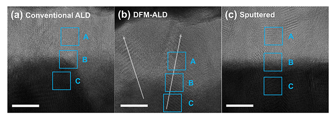
1-2) Discrete feeding method (DFM)
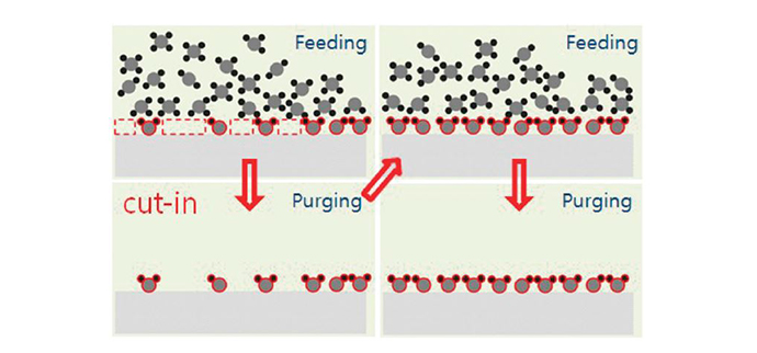
- To achieve an ideal growth behavior of the Ru films, a discrete feeding method (DFM)-ALD process was adopted. The DFM-ALD was performed by dividing the Ru feeding and purge steps of the conventional ALD process into several steps (shorter feeding/purge time) with an identical total feeding/purge time. The DFM-ALD removed the physisorbed precursor and byproduct molecules effectively through the cut-in purge steps. As a result, nucleation characteristics were improved, resulting in the uniform growth of the Ru films.
- Furthermore, the physicochemical properties of the Ru films, such as a preferred orientation could be optimized for the deposition of the upper dielectric films. Consequently, an improvement in the electrical performance of the MIM capacitor was obtained.
Related Papers :
- J. H. Han et al. "Chemical Vapor Deposition of Ru Thin Films with an Enhanced Morphology, Thermal Stability, and Electrical Properties Using a RuO4 Precursor." Chem. Mater, 21.2, 207-209 (2009)
- J. H. Han et al. "Growth of RuO2 Thin Films by Pulsed-Chemical Vapor Deposition Using RuO4 Precursor and 5% H2 Reduction Gas." Chem. Mater, 22.20, 5700-5706 (2010)
- T. J. Park et al. "Improved Growth and Electrical Properties of Atomic-Layer-Deposited Metal-Oxide Film by Discrete Feeding Method of Metal Precursor." Chem. Mater, 23.7, 1654-1658 (2011)
- C. H. An et al. "Substrate Effects on the Growth Behavior of Atomic-Layer-Deposited Ru Thin Films Using RuO4 Precursor and N2/H2 Mixed Gas." J. Phys. Chem. C, 123.36, 22539-22549 (2019)
- D. S. Kwon et al. "Atomic layer deposition of Ru thin films using (2,4-dimethyloxopentadienyl) (ethylcyclopentadienyl)Ru and the effect of ammonia treatment during the deposition." J. Mater. Chem. C, 8.21, 6993-7004 (2020)
- D. S. Kwon, et al. "Improved Properties of the Atomic Layer Deposited Ru Electrode for Dynamic Random-Access Memory Capacitor Using Discrete Feeding Method." ACS Appl. Mater. Interfaces, 13(20), 23915-23927 (2021)
Related research group homepage
- http://thinfilm.seoultech.ac.kr - Prof. Jeong Hwan Han
- http://nel.hanyang.ac.kr - Prof. Tae Joo Park
2. TiO2 dielectric thin films
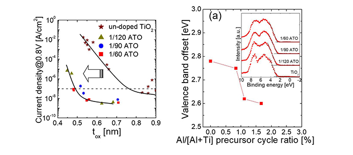
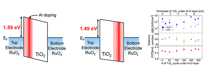
2-1) Deposition of Al-doped TiO2 dielectric thin films with ALD method- Titanium oxide (TiO2) was highlighted as the next generation DRAM dielectric material due to its high dielectric constant (~40 for anatase and ~100 for rutile phase). However, the high leakage current density of TiO2 film is highly problematic compared to other binary oxides such as ZrO2 and HfO2 due to its small bandgap (~3.1 eV) and n-type nature. To suppress leakage current, Al ions were doped in TiO2 film. Doped Al atoms function as an acceptor in TiO2 film, suppressing leakage current. As a result, tox of ~0.5 nm was achieved while maintaining a low enough leakage current density.
2-2) Electrical properties of Al-doped TiO2 films depending on the Al-doping profile
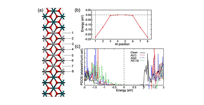
- Al ions in TiO2 film work as acceptors and increase the conduction band offset (CBO), therefore increasing the Schottky barrier height. Since the energy level of the Al dopant site is located below the middle level of the bandgap of TiO2, Al ion doping results in Fermi energy level lowering and increases CBO. It was discovered that locating the Al2O3 ALD cycle near the top and bottom interfaces could more efficiently suppress leakage current since interface state-dependent Schottky emission is the main leakage conduction mechanism in the lower voltage regions. Moreover, it was discovered that keeping Al concentration as low as possible is crucial for reducing dielectric loss.
Related Papers :
- S. K. Kim et al. "Al-Doped TiO2 Films with Ultralow Leakage Currents for Next Generation DRAM Capacitors." Adv. Mater, 20.8, 1429-1435 (2008)
- W. Jeon, et al. "Controlling the Al-Doping Profile and Accompanying Electrical Properties of Rutile-Phased TiO2 Thin Films." ACS Appl. Mater. Interfaces, 6, 7910-7917 (2014)
- W. Jeon, et al. "Asymmetry in electrical properties of Al-doped TiO2 film with respect to bias voltage." Phys. Stat. Solidi-Rapid Research Letters, 9, 410-413 (2015)
Related research group homepage
- http://lete-khu.kr/ - Prof. Woojin Jeon
3. SrTiO3 dielectric thin films
3-1) SrTiO3 dielctric thin films- Strontium titanate (SrTiO3, STO) dielectric film, which has a very high bulk dielectric constant (~300), is being studied for the next generation of DRAM capacitors. STO thin films were grown on Ru substrates by ALD method, which consisted of several alternating SrO and TiO2 cycles. Controlling the cation stoichiometry, which was difficult because of the oxygen-scavenging property of SrO at initial growth, was the key factor for the enhancement of electrical and dielectric properties. Varying ALD precursors was one method to control non-ideal growth at the early stages of film growth without increasing process complexity.
- Using less-reactive {Sr(demamp)(tmhd)}2 as Sr-precursor suppressed the excessive growth of SrO at the initial stage and enhanced stoichiometry. However, the limitation in mass production arises due to the difficulty of synthesis. Therefore, another method is to change Ti-precursor to Ti(Me5Cp)(OMe)3, which has a higher reactivity with oxidized Ru substrate. As a result, fewer surface oxygens reacted with the Sr atoms, suppressing the excessive growth at the initial stage and enhancing stoichiometry.
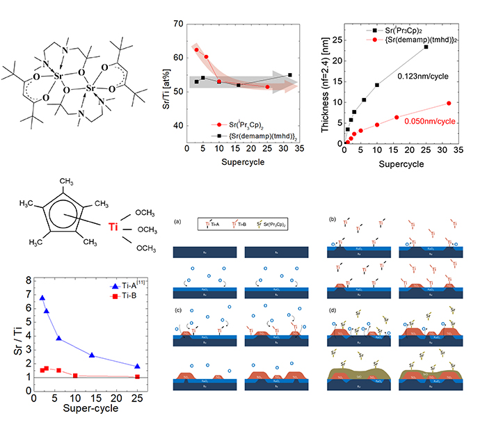
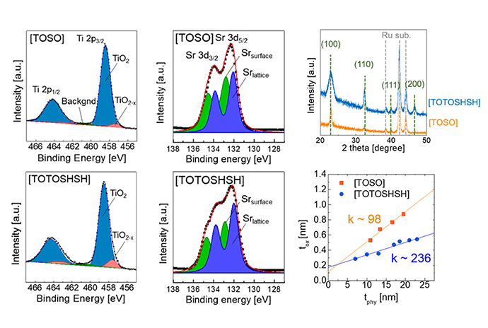
3-2) Analysis of the incorporation behaviors of Sr and Ti atoms in SrTiO3 films
- The precursor incorporation behavior of STO is largely affected by the physical and chemical circumstances in ALD sub-cycles (Sr-O cycle or Ti-O cycle), and differences in incorporation behavior can result in STO film electrical property variations. When O3 or H2O was adopted as the oxygen source for the Sr-O sub-cycles, the incorporation rate of the Ti precursors almost doubled. Also, crystallization was enhanced when O3 was used rather than H2O. Results indicate that careful controlling of the ALD process conditions for STO deposition is crucial.
Related Papers :
- S. W. Lee et al. "Atomic Layer Deposition of SrTiO3 Thin Films with Highly Enhanced Growth Rate for Ultrahigh Density Capacitors." Chem. Mater, 23.8, 2227-2236 (2011)
- W. Lee et al. "Colloidal Photonic Crystals toward Structural Color Palettes for Security Materials." Chem. Mater, 25, (2013)
- W. Lee et al. "Improved Initial Growth Behavior of SrO and SrTiO3 Films Grown by Atomic Layer Deposition Using {Sr(demamp)(tmhd)}2 as Sr-Precursor." Chem. Mater, 27, (2015)
- M. J. Chung et al. "Quantitative Analysis of the Incorporation Behaviors of Sr and Ti Atoms During the Atomic Layer Deposition of SrTiO3 Thin Films." ACS Appl. Mater. Interfaces, 10, 10, 8836-8844 (2018)
- S. H. Kim et al. "Effect of Growth Temperature during the Atomic Layer Deposition of the SrTiO₃Seed Layer on the Properties of RuO2/SrTiO3/Ru Capacitors for Dynamic Random Access Memory Applications." ACS Appl. Mater. Interfaces, 10, 48, 41544-41551 (2018)
Related research group homepage
- http://nfml.ajou.ac.kr - Prof. Sang Woon Lee
- http://nfml.ajou.ac.kr - Prof. Woongkyu Lee
4. BeO and MgO dielectric thin films
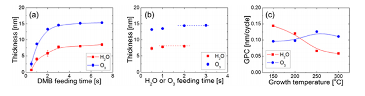
4-1) BeO dielectric thin films- Beryllium oxide (BeO) has a very large bandgap of 10.6 eV, even larger than that of SiO2 (~9 eV). Growth characteristics and properties of BeO films grown by atomic layer deposition (ALD) were investigated. ALD chemistries between dimethylberyllium and two different oxygen sources, H2O and O3, were governed by different reaction mechanisms, resulting in different film properties. At growth temperatures ranging from 150 to 300 °C, the properties of the BeO films grown using H2O were temperature independent. In contrast, the BeO films grown using O3 at low temperatures (<200 °C) showed high concentrations of carbon and hydrogen, possibly owing to the incomplete removal of the ligands of the precursor, resulting in low film density. These findings demonstrate that the O3-ALD process requires relatively more thermal energy than the H2O-ALD case to produce high-quality BeO films.
4-2) MgO dielectric thin films
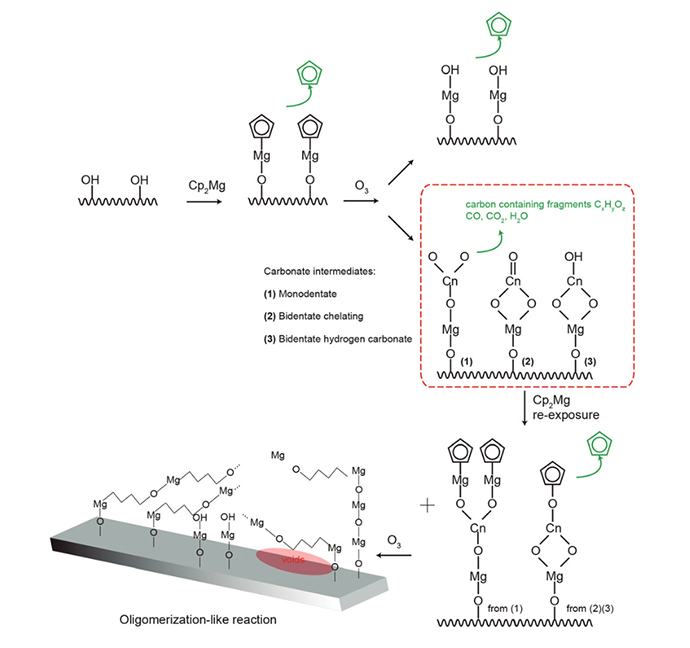
- Magnesium oxide (MgO) has a bandgap of 7.3 eV and a dielectric constant value of ~10, which may supplement the weakness of the amorphous Al2O3 for applications requiring high capacitance and low leakage current. It could also trigger the BeO film phase transition to a cubic phase. The dissimilarities of MgO thin film growth mechanisms were comparatively studied via ex-situ techniques in the ALD process with O3 or H2O as the oxygen source. The bis(cyclopentadienyl)magnesium [Mg(Cp)2] was adopted as the Mg-precursor. The insufficient H2O purging time caused the Mg hydrides to remain in the deposited MgO thin film and inhibited growth on Si substrate. However, an abnormal overgrowth zone around 290 °C in MgO O3 ALD on the Si substrate was found. Oligomerization may have happened between ligands after the Cp ring rupture, causing void formation, low density, and a relatively high impurity level. Substrate temperature could greatly affect the growth behaviors, film properties as well as film-based MIM devices.
Related Papers :
- W. C. Lee et al. "Growth and Characterization of BeO Thin Films Grown by Atomic Layer Deposition Using H2O and O3 as Oxygen Sources." J. Phys. Chem. C, 121, 17498-17504 (2017)
- W. C. Lee et al. "Atomic engineering of metastable BeO6 octahedra in a rocksalt framework." Surface Science, 501, 144280 (2020)
- B. Wang et al. "Influences of oxygen source and substrate temperature on the unusual growth mechanism of atomic layer deposited magnesium oxide using bis(cyclopentadienyl)magnesium precursor." J. Mater. Chem. C, 9.42, 15359-15374 (2021)
5. ZrO2 dielectric thin films
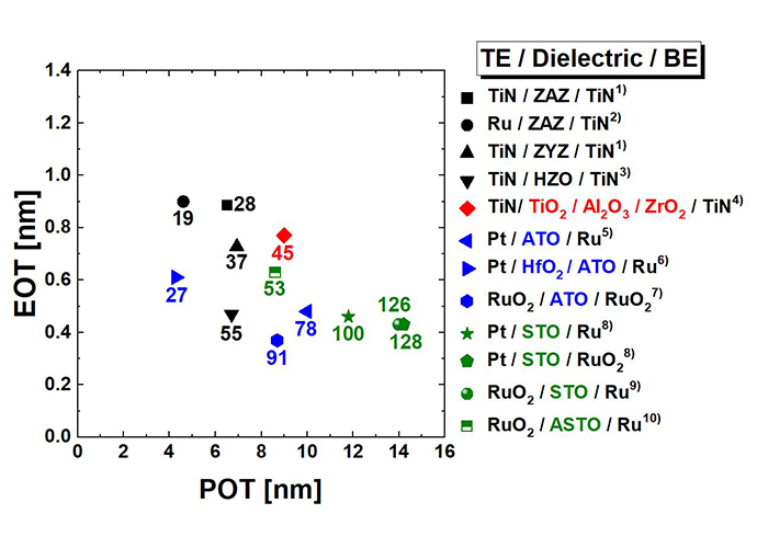
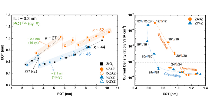
5-1) Crystallization behavior of ZrO2/Y2O3/ZrO2 dielectric thin films- Crystallization behaviors of ALD-grown ZrO2/Y2O3/ZrO2 (ZYZ) and ZrO2/Al2O3/ZrO2 (ZAZ) thin films have been investigated for further scaling of the next generation DRAM capacitor. The Al2O3 insertion layer required for leakage current suppression degraded the overall crystallinity of the ZrO2 film. The EOT-POT plot clearly indicated that the Al2O3 layer impeded the progress of ZrO2 grain growth. Conversely, the impact of the Y2O3 insertion layer on the crystallization of ZrO2 was almost negligible, resulting in a similar EOT change as the pure ZrO2 case. The leakage current density suppression, comparable to that of the ZAZ film, was still observed with the ZYZ film.
Related Papers :