 HOME > Research > Ferroelectric
Ferroelectric
Ferroelectric research
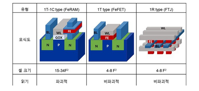
- Ferroelectric materials are characterized by two stable polarization states that can be switched by applying an electric field. Because ferroelectric materials maintain a polarized state after removing the electric field, the application of ferroelectric materials in nonvolatile memories has attracted much attention. Memory using ferroelectricity is largely classified into three categories; measuring the charge related current when an electric field is applied to the capacitor (FeRAM), measuring the Vth shift of transistor caused by unscreened polarization charge of the ferroelectric layer (FeFET), measuring the tunneling current in very thin ferroelectric layer (FTJ).
- M. H. Park, et al, “Renaissance of Ferroelectric Memories: Can they be a game-changer?”, KPS (2021)
1. (Hf, Zr)O2 ferroelectric materials
- Recently, it was reported that HfO2 show robust ferroelectric (FE) properties when doped with various dopants such as Zr, Si, Y, Al, Gd, La, and Sr. Compared to the conventional ferroelectrics based on perovskite or layered perovskite structure, such as Pb(Zr,Ti)O3 and SrBi2Ta2O9, the FE HfO2-based films showed quite distinctive physical and electrical properties. The HfO2-based films can be extremely thin (film thickness, tf < 10 nm) with feasible ferroelectricity (remnant polarization, Pr ~ 10-40 μC/cm2), whereas the much thicker thicknesses (tf > 100 nm) are required for the stable FE properties of conventional ferroelectrics thin films, especially with the metal-ferroelectric-metal (MFM) configuration. Due to their small thickness, the HfO2-based films are considered promising for the three-dimensional capacitor structure, which is highly required for the future ferroelectric random-access-memory (FeRAM) device according to International Technology Roadmap for Semiconductors. This results from the relatively large bandgap (Eg ~ 5.5 eV), high compatibility with Si, and matured atomic layer deposition (ALD) technique of HfO2-based films. In fact, due to their high Si-compatibility, the non-FE HfO2 thin film has been used as the buffer layer in ferroelectric field-effect-transistor (FeFET) to solve the interfacial problems of conventional ferroelectrics and Si substrate.
1-1) HZO Thin film (polar phase & electrical properties)
- A-IGZO TFTs induce severe instability under negative bias temperature stress, reflecting the importance of studying the effect of light illumination on TFTs.
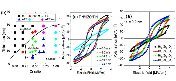
- We examined the effect of tf on the FE properties of the Hf0.5Zr0.5O2 films. They tested the Hf0.5Zr0.5O2 (HZO) films with various tf (5.5-25 nm) and annealing temperatures (400-800 °C). When the tf was ≈ 10 nm, the Pr of the Hf0.5Zr0.5O2 films was the largest (≈ 15 μC cm-2), whereas the Pr decreased to ≈ 12 and ≈ 5 μC cm-2 when the tf increased to 17 and 25 nm, respectively. This could be understood from the fact that the portion of m-phase increased as the tf increased. Meanwhile, we also found that the insertion of thin (~1nm) dielectric Al2O3 inter-layer between 20-nm- thick Hf0.5Zr0.5O2 layers can prevent the continued growth of the whole Hf0.5Zr0.5O2 films, and the FE properties were not degraded with increasing tf.
- The origin of the formation of an unexpected FE phase was systematically examined for Hf0.5Zr0.5O2 films by our group. Since the growing nuclei are supposed to have t-phase structure prior to the zipping, and because of the surface energy effect, there must be several variations in the resulting strain states after the zipping, according to the original crystallographic directions of the nuclei. Using the in-plane stress condition of the film, we could calculate the strain along the a-, b-, and c-axis of the grains of various orientations using the in-plane stress conditions of the thin film. As a result, the 110- orientation was the most favorable for forming the o-phase from the t-phase, whereas the 111- orientation was the worst since almost equivalent strains were formed along the a-, b-, and c-axis.
Related Papers :
- M. H. Park, et al. "Ferroelectricity and Antiferroelectricity of Doped Thin HfO2-Based Films." Advanced Materials, 11, 27, 1811-1831 (2015).
- M. H. Park, et al. "The effects of crystallographic orientation and strain of thin Hf0.5Zr0.5O2 film on its ferroelectricity." Appl. Phys. Lett. 104, 072901 (2014).
- H. J. Kim, et al. "Grain size engineering for ferroelectric Hf0.5Zr0.5O2 films by an insertion of Al2O3 interlayer." Appl. Phys. Lett. 105, 192903 (2014).
- M. H. Park, et al. "Study on the degradation mechanism of the ferroelectric properties of thin Hf0.5Zr0.5O2 films on TiN and Ir electrodes." Journal of Applied Physics, 111, 024511 (2012)
- (서울대학교 재료공학부 박민혁 교수 - https://sites.google.com/view/neemlab)
1-2) Wake Up Effect of HZO Thin Film
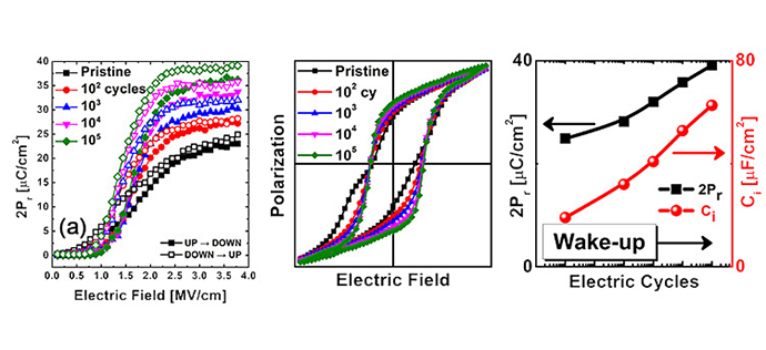
- The Hf0.5Zr0.5O2 film shows mostly ferroelectric (FE)-like behavior in the pristine state, where the slight anti-ferroelectric (AFE)-like distortion could be ascribed to the antiparallel distribution of some of the FE domains and the AFE phase. The field cycling of only 100 cycles almost completely removed such antiparallel pinned domains. Further increase in the field cycling number more effectively poled the domains making the Pr increase significantly. Field cycling also transformed the non-FE phases, mostly at the electrode interface, to the FE phase, which could be inferred from the increase in the interfacial capacitance. These results indicate that the physical state of the FE-phases in the HZO film is quite different from the conventional FE thin films, such as PZT, in the sense that it is the outcome of variously oriented domains, possibly including antiparallel orientation. Field cycling plays a role in poling in conventional FE materials, but the high field-induced non-FE t-phase to FE o-phase transition could also contribute to the effective poling (depinning of the pinned FE domains).
Related Papers :
- H. J. Kim, et al. "A study on the wake-up effect of ferroelectric Hf0.5Zr0.5O2 films by pulse-switching measurement." Nanoscale, 8, 1383-1389 (2016)
- Park, Min Hyuk, et al. "Effect of Zr Content on the Wake-Up Effect in Hf1-xZrxO2 Films." ACS applied materials & interfaces 8.24 (2016).
- Park, Min Hyuk, et al. "Study on the size effect in Hf0.5Zr0.5O2 films thinner than 8nm before and after wake-up field cycling." Applied Physics Letters 107.19 (2015)
1-3) Ferroelectric switching in a ferroelectric - dielectric bilayer
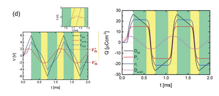
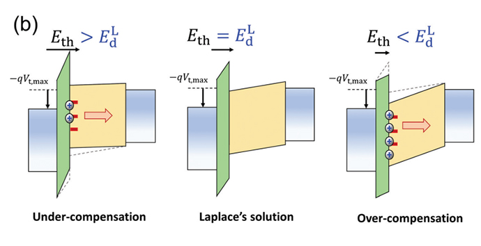
- Ferroelectric random access memory devices (FeRAM) have attracted a great deal of interest as a potential replacement for nonvolatile stand-alone memory devices or as a memory element in a system-on-chip device where a high density (> 16 mega bit) is preferred for the device performance and cost-effectiveness. However, scaling down the ferroelectric thin films has some practical problems. One of them is that Interfacial effects become increasingly severe as the ferroelectric layer thickness decreases, which has made ultra-thin ferroelectric film applications virtually impractical. It was confirmed experimentally that non-ferroelectric interlayers have detrimental effects on the FE functionality of thin film. On the contrary, we observed that an interfacial layer could be used positively. It is possible that this interfacial layer (tunnel switch layer) can be utilized constructively to improve the reliability of a FE capacitor if by-electrode charge injection is blocked by this layer. And also, it opens up during FE switching, minimizing the adverse interference with FE switching, but closes during the non-switching or post switching overvoltage stress, improving the reliability of a FE capacitor.
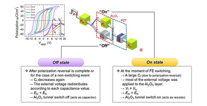
- We also presented the dynamic model to simulate the whole process of injection involved in switching in the bilayer structure. Moreover, we could separate the injected charge and ferroelectric polarization via pulse measurement of the MFMDM device. Through this separation technique, quantitative analysis of the injection charges apart from the ferroelectric bound charge was acquired. Most notably, it was found that the overly injected charges compared to polarization resulted in the over-compensation condition, which improved the retention of the bilayer structure. It was found that the degree of compensation was determined by the applied bias condition and the material properties of the dielectric layer.
Related Papers :
1-4) Enhanced properties in Hf0.5Zr0.5O2 films using interfacial layer
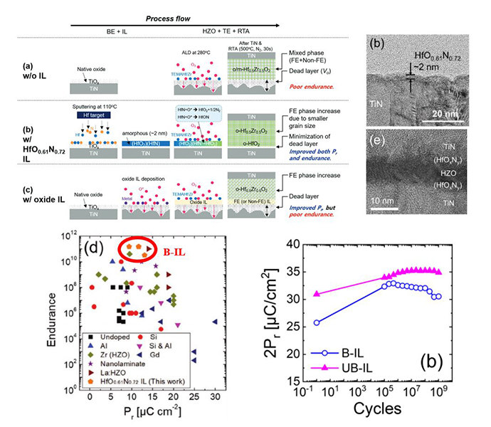
- TiN is the primary electrode material for doped HfO2 FE thin films. However, TiN is vulnerable to oxidation, resulting in the production of the non FE TiOx interlayer. Such an interfacial layer formed between TiN electrode and HZO film degrades the reliability of the HZO. In this regard, the nitride interlayer could improve the reliability of HZO and reduce the depolarization effect.
- We deposited a thin HfOxNy layer (~2nm) on the BE TiN surface, and the Pr was enhanced by 33% compared with the case without an interfacial layer. The B-IL also suppressed the grain growth and the undesirable monoclinic phase in the HZO film, which showed an endurance of up to 1.5 x 10¹¹ times
- On the other hand, when we deposited a thin HfOxNy layer between the top electrode and HZO film, it showed a larger average grain size. Nonetheless, there remained a trace amount of nitrogen at the TE interface, which could decrease the portion of the m-phase. Consequently, the Pr was enhanced, and there was no degradation in Pr for up to 109 cycles. Above researches proved that the interfacial engineering is pivotal in optimizing ferroelectric properties in MFM / MFS devices
Related Papers :
- Kim, Beom Yong, et al. "Enhanced Ferroelectric Properties in Hf0.5Zr0.5O2 Films Using a HfO0.61N0.72 Interfacial Layer." Advanced Electronic Materials (2021)
- Kim, Beom Yong, et al. "Improved ferroelectricity in Hf0.5Zr0.5O2 by inserting an upper HfOxNy interfacial layer." Applied Physics Letters 119.12 (2021)
2. Application of HfO2 based ferroelectric materials
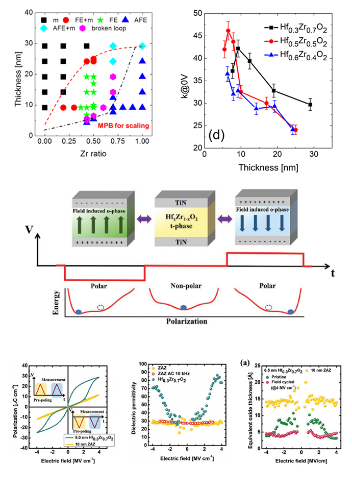
2-1) Hf1-xZrxO2 thin films for high k dynamic random access memory- As the cell capacitance of DRAM decreases with aggressive scaling down of the cell size, dielectric materials with a higher dielectric permittivity (k) are needed to store sufficient charges for operation. However, high k materials are known to have problems such as noble metal electrodes and significant leakage current.
- The utilization of MPB between the orthorhombic phase and the tetragonal phase in an HfO2-ZrO2 solid solution is suggested for a high capacitance dielectric capacitor. These films showed increasing k values with decreasing film thickness. Among them, Hf0.5Zr0.5O2 and Hf0.3Zr0.7O2 films showed 47, 43 k values at 6.5, 9.2nm thicknesses. Through the optimization of the annealing process, a 0.62 nm equivalent oxide thickness was reported for the 6.5nm thick Hf0.5Zr0.5O2 film.
- And also, HZO showed field-induced ferroelectric characteristics that enable large reversible polarization change, which makes it promising for DRAM capacitive layer. So we investigated reversible transition between the non-polar t- and field-induced polar o- phases in the HZO film for the DRAM application. The charging and discharging behaviors upon DC pulsed voltage were investigated, and 6.5nm Hf0.3Zr0.7O2 showed FFE characteristics at an applied field ~ 2.5MV/cm. And it showed k value as high as ~80 under 4MV/cm DC pulse field which is too high electric field to operate normal DRAM. However, the film showed a reduced critical field with decreasing Zr contents so that a k value of 60~80 could be obtained in the low electric field (0~2MV/cm), and an EOT of 0.47nm was achieved with a stable leakage current at DRAM operating voltage. (0.8V)
Related Papers :
- Hyun, Seung Dam, et al. "Dispersion in Ferroelectric Switching Performance of Polycrystalline Hf0.5Zr0.5O2 Thin Films." ACS applied materials & interfaces 10.41 (2018)
- Park, Min Hyuk, et al. "Morphotropic Phase Boundary of Hf1-xZrxO2 Thin Films for Dynamic Random Access Memories." ACS applied materials & interfaces 10.49 (2018)
- Hyun, Seung Dam, et al. "Field-Induced Ferroelectric Hf1-xZrxO2 Thin Films for High-k Dynamic Random Access Memory." Advanced Electronic Materials 6.11 (2020)
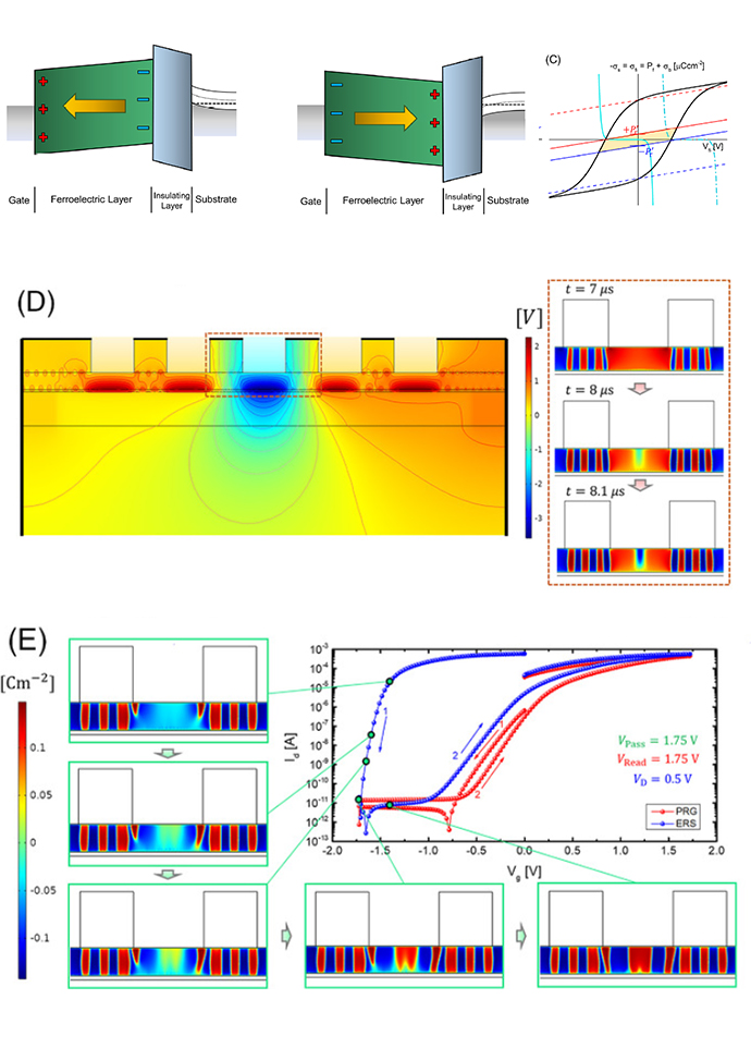
2-2) Ferroelectric field-effect transistors for three-dimensional storage applications
- FeFET fundamentally operates based on the principle that the uncompensated FE bound charge induces an electric field effect on the semiconductor channel. The use of FeFET has been highlighted because of its one transistor configuration with low operation voltage. It encounters several issues due to the inevitable involvement of the depolarization effect. Ironically the depolarization effect is the fundamental source of the field-effect of FEFET. In this sense, a critical issue is striking a balance between desirable (memory window) and undesirable (FE bound charge loss) outcomes by tuning the material parameters.
- We proposed the simple 1D load line analysis method to understand the basic feature of FeFET operation. According to the 1D load line analysis, the necessary material properties that will allow for sufficient device performance are sufficiently large Vc (>3V), moderate Pr (1-2μCcm-2), and the presence of a highly insulating interfacial high k dielectric layer.
- We further developed the 2D/3D simulation packages to model the dynamics of the multidomain structure in FeFET. The 2D/3D simulations of the prototypical ferroelectric-NAND (FE-NAND) string indicate that the field interference effect could be severe if the device geometry and operational voltage scheme are not optimized. Even the favorable hypothetical material properties assumed in this work posed a significant interference problem, which caused 30-40% of the Vth of a programmed cell to shift into the erased state.
- In general, conventional ferroelectric materials have too high Pr and too low Vc to make a useful FeFET, so further investigation of new ferroelectric and dielectric materials is necessary. In this regard, the recent finding of very high Ec materials such as Al(Sc)N is eye-catching.
Related Papers :
2-3) Negative capacitance in ferroelectric thin films
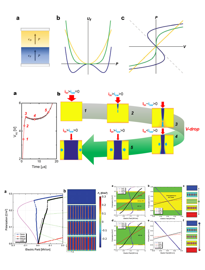
- MOSFET is operated by the modulation of the semiconductor channel potential, of which the performance is usually assessed by the subthreshold swing (SS) value. Negative capacitance (NC) in the ferroelectric thin film has attracted a lot of attention in order to decrease SS. When FE is in the NC state (depoled state P=0) gate insulator (GI) works as the internal voltage booster. Nonetheless, it corresponds to an energetically unstable state, so maintaining the depoled state is highly challenging.
- It was assumed that simple stacking of DE and single domain FE could stabilize the NC state of the FE layer. When the FE layer is in the NC state, (differential) voltage across the DE layer must increase over the (differential) applied voltage, which results in the enhancement of the stored charge within the metal electrode over the single DE. However, in reality, FE mostly exists in a multidomain state rather than in the depoled state, so it is hardly expected that DE/multidomain FE can show NC behavior. Nonetheless, we observed V drop effect from the 150nm thick epitaxial BaTiO3, which was analyzed based on the conventional domain switching model of the KAI formalism. Apart from the claim on the emergence of NC effect in a PZT film which showed V drop effect, we unveiled that the V drop can be explained by the mismatch between the influx of charge flow and its consumption by the reverse domain formation in the FE capacitor. We also elucidated that the quasi-static NC operation can be possible in multidomain FE by extensive numerical simulation.
- Movie 1 shows the time-dependent evolution of the domain when the external field increases from 0 to 0.2MV/cm. It is confirmed that a slope of the Pf - Ef curve is negative during the lateral DW motion until the saturation to the single domain occurs. In movie 2, while the potential across the top and bottom DE layers is always increased, the potential across the middle FE layer temporarily decreased with increasing Vapp. This voltage amplification disappears when the FE film becomes fully polarized.
- And we examined the full FE switching behavior of the MIFIM system. When the FE film was thick enough in the MIFIM (or MFIM) structure (~85nm), unlike the prior lateral growth of the stripe domains, the FE switching was dominantly accomplished by domain nucleation and growth. This switching is accompanied by a significant internal voltage boosting, which corresponds to the transient NC effect but involves a significant hysteresis. As the FE film became thinner, stripe domain structure which can show (quasi-) static NC effect with minimal involvement of the hysteresis effect, was achieved. Under the optimized condition, which corresponds to the case with the FE film thickness being near the critical thickness (~10nm), operation voltage range being consistent with the stripe domain configuration, and voltage drive speed being lower than the DW migration speed, the MIFIM can show hysteresis-free static NC behavior. The FE film with a thickness lower than the FE-stabilization limit (~6nm) is homogeneously depolarized near E = 0, and PF - EF curve in this region precisely follows the S curve from the LGD theory meaning that MIFIM remained at the static intrinsic NC state. When Eapp increases, the stripe domains were formed, and then the FE film becomes fully polarized which corresponds to the PC state. Through this simulation, we found out that quasi-static NC could be achieved within a limited parameter space even when the FE switching is mediated by the multidomain structure.
Related Papers :
- Park, Hyeon Woo, et al. "Negative capacitance from the inhomogeneous stray field in a ferroelectric-dielectric structure", Adv. Funct. Mater. 2200389 (2022)
- Park, Hyeon Woo, et al. "Modeling of Negative Capacitance in Ferroelectric Thin Films." Advanced Materials 31.32 (2019)
- Kim, Keum Do, et al. "Transient Negative Capacitance Effect in Atomic-Layer-Deposited Al2O3/Hf0.3Zr0.7O2 Bilayer Thin Film." Advanced Functional Materials 29.17 (2019)
- Kim, Yu Jin, et al. "Voltage Drop in a Ferroelectric Single Layer Capacitor by Retarded Domain Nucleation." Nano letters 17.12 (2017)
- Kim, Yu Jin, et al. "Time-Dependent Negative Capacitance Effects in Al2O3/BaTiO3 Bilayers." Nano letters 16.7 (2016)
- Kim, Yu Jin, et al. "Alternative interpretations for decreasing voltage with increasing charge in ferroelectric capacitors." Scientific reports 6.1 (2016)