 HOME > Research > Resistive Switching Memory
Resistive Switching Memory
Resistive switching memory research
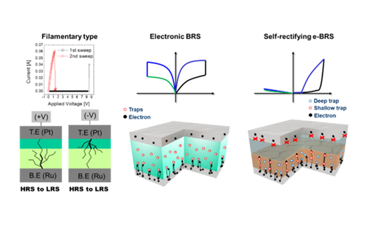
- Rapid advances in information technology rely on high-speed and large-capacity nonvolatile memories. Several alternatives to recent Flash memory have been extensively studied to obtain a more powerful and functional nonvolatile memory. We review the current status of one of the alternatives, resistance random access memory (ReRAM), which uses a resistive switching phenomenon found in transition metal oxides. A ReRAM memory cell is a capacitor-like structure composed of insulating or semiconducting transition metal oxides that exhibits reversible resistive switching on applying voltage pulses. Recent advances in understanding the driving mechanism are described in light of experimental results involving memory cells with filamentary, e-BRS, and self-rectifying e-BRS.
1. Device and mechanism study
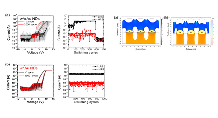
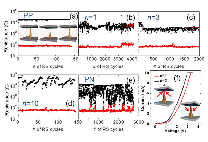
1-1) Nano-dot device- The conventional resistive switching RAM (ReRAM) can exhibit analog-type switching due to its inherent carrier ion migration. However, due to the randomness of the migration, not-so-stable states are a critical problem to be used in practical applications. One way to break through this problem is the enhancement of the electric field between electrodes, which can be obtained from the insertion of the nanostructure such as Cu cone or Au nanodot structure. Our group is focused on developing the stable analog-type ReRAM using self-rectifying BRS with the nanostructure. Such that the cell-to-cell variation, endurance, and cycle-to-cycle variation can be improved in the cross-bar array (CBA) structure on a larger scale.
1-2) Cu-cone device
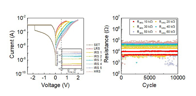
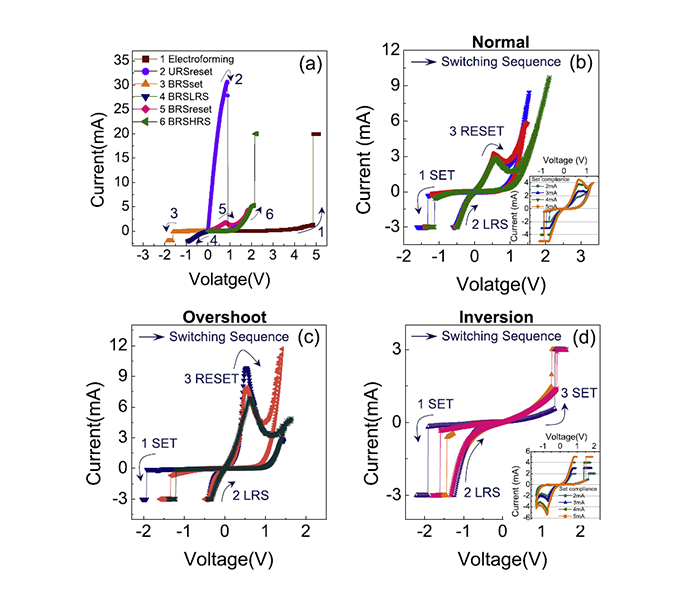
- Memristor is considered one of the key components of neuromorphic hardware aiming to overcome the limitations of classical von Neumann computers, but the continuous control of the device conduction remains a challenge. Random and stochastic dynamics of weak conducting filaments (CF) hinder the precise control of the resistance states, particularly in the conductive bridge random access memory (CBRAM). The problem of random and stochastic resistive switching of the Cu-based CBRAM is largely mitigated by inserting the Cu-cone as a cation source into the memory cell (Cu-cone device). The electric field concentrated on the Cu-cone induces stronger CF with a limited number near the tip region, making the device feature distinctive from the planar Cu CBRAM. The Cu-cone device exhibits enhanced resistance controllability attributed to the well-controlled CF, improved switching reliability improvement, and multiple intermediate resistance states. Such features are used to explore its usefulness as an artificial synapse, where fluent potentiation and depression can be achieved using voltage pulses. Further research is still required to emulate the artificial synapses fully, but the feasibility is presented in this work by exploiting the similarities between the Cu cations in the CBRAM device and the Ca2+ dynamics in a biological synapse.
Related Papers :
- J. H. Yoon et al. "Uniform Self-rectifying Resistive Switching Behavior via Preformed Conducting Paths in a Vertical-type Ta2O5/HfO2-x Structure with a Sub-μm2 Cell Area." ACS Appl. Mater. Interfaces, 8 (2016).
- H. J. Kim et al. "Fabrication of a Cu-Cone-Shaped Cation Source Inserted Conductive Bridge Random Access Memory and Its Improved Switching Reliability." Adv. Funct. Mater. 1806278 (2019).
- H. J. Kim et al. "Multilevel Control of Conductive Filament Evolution and Enhanced Resistance Controllability of the Cu-Cone Structure Embedded Conductive Bridge Random Access Memory." Adv. Electron. Mater. 2100209 (2021).
1-3) Electronic Binary Resistive Switching (e-BRS)
- The resistance state of electronic binary resistive switching (e-BRS) devices can be modulated by trapping and detrapping the electrons in the dielectric switching layer. Since the electronic switching mechanism doesn’t involve ionic migration, they have better memory capabilities such as lower power consumption, better endurance, and a higher switching speed compared with the ionic switching mechanism. By selecting the appropriate electrode materials and the stack of dielectric switching layers, various switching characteristics suitable for high-density memory applications such as self-compliance and self-rectification can be obtained.
Related Papers :
- J. H. Yoon et al. "Highly Uniform, Electroforming-Free, and Self-Rectifying Resistive Memory in the Pt/Ta2O5/HfO2-x/TiN Structure." Adv. Funct. Mat. 24.32: 5086-5095 (2014).
- J. H. Yoon et al. "Pt/Ta2O5/HfO2-x/Ti Resistive Switching Memory Competing with Multilevel NAND Flash." Adv. Mater., 27, 3811 (2015).
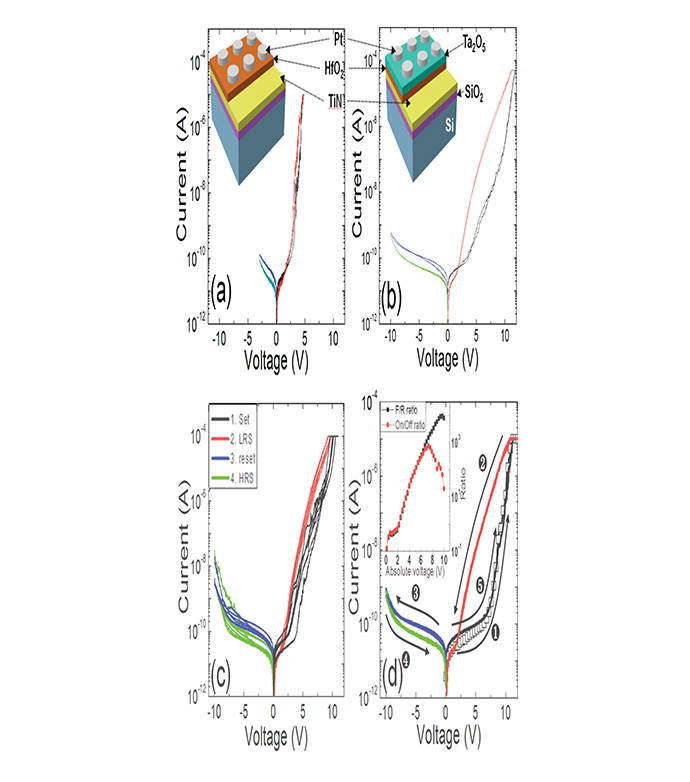
- J. H. Yoon et al. "The current limit and self-rectification functionalities in the TiO2/HfO2 resistive switching material system." Nanoscale 9.33, 11920-11928 (2017).
Related research group homepage
- https://emdslab.wixsite.com/emds/pi - Dr. Jung Ho Yoon
1-4) Mechanism study of ReRAMs
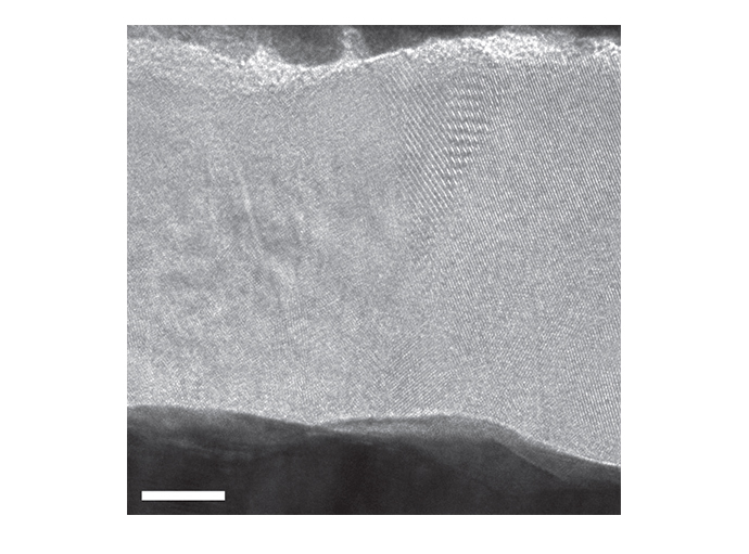
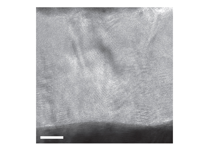
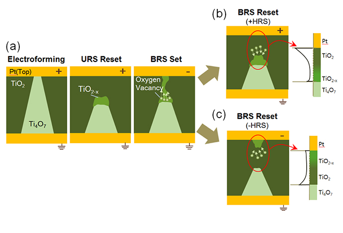
- Since the first demonstration of a resistive switching device, many studies have focused on revealing the underlying mechanism of resistive switching. Yet, the mechanism which can universally explain the origin of resistive switching has not been suggested. Still, progress has been made in investigating the switching mechanism and various switching modes of TiO2-based ReRAMs. It was verified that the Magneli phase (TinO2n-1, n≥4) transition plays a crucial role in the RS operation mechanism in TiO2-based RS memories through extensive high-resolution transmission electron microscopy and electron diffraction analyses. It was the very first time that conductive filaments were observed directly. Moreover, suitable switching steps targeted for reliable memory applications were investigated.
Related Papers :
- D. H. Kwon et al. "Atomic structure of conducting nanofilaments in TiO2 resistive switching memory." Nature nanotechnology, 5(2), 148-153 (2010).
- K. J. Yoon et al. "Memristive tri-stable resistive switching at ruptured conducting filaments of a Pt/TiO2/Pt cell." Nanotechnology, 23(18), 185202 (2012).
- G. H. Kim et al. "Improved endurance of resistive switching TiO2 thin film by hourglass shaped Magneli filaments." Applied physics letters, 98(26), 262901 (2011).
- K. J. Yoon et al. "Ionic bipolar resistive switching modes determined by the preceding unipolar resistive switching reset behavior in Pt/TiO2/Pt." Nanotechnology, 14, 24, 145201 (2013).
Related research group homepage
- FuST Research. - Future Semiconductor Technology laboratory (kaist.ac.kr) - Prof. Kyung Min Kim
2. 3D-NAND-like VRRAM, Vertical TFT ReRAM
- Vertical ReRAM can overcome the planar scalability limits and further increase memory density. There are many suggestions on viable structures of V-ReRAM, and 3D-NAND-like hole structure is favored due to ease of fabrication process and less peripheral area over multilayer stacked planar CBA. Increased cell density in V-ReRAM can cause a harsher sneak current problem than planar CBA, requiring better selector performance. Introducing an active selector (TFT) to each cell can effectively block sneak current. This Vertical TFT ReRAM (V-TFT-ReRAM) structure also allows compatibility with the conventional NAND operation scheme.
- V-TFT-ReRAM consists of strings of parallel TFTs and resistors. On-channel TFTs become electrodes for the selected resistor and drive voltage. For fluent circuit operation, the resistance of TFT should be far below (when on) or above (when off) the RS range of resistor, as an equivalent resistance of the whole string, is read.
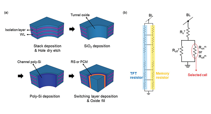
- To realize V-TFT-ReRAM, compatibility of TFT and resistor, required scale for each component, viability of sidewall switching, etc. are in evaluation.
Related Papers :
- J.Y. Seok et al. "A Review of Three-Dimensional Resistive Switching Cross-Bar Array Memories from the Integration and Materials Property Points of View." Adv. Funct. Mater. 24, 5316-5339 (2014).
- K.J. Yoon et al. "What Will Come After V-NAND-Vertical Resistive Switching Memory?" Adv. Electron. Mater. 5, 1800914 (2019).
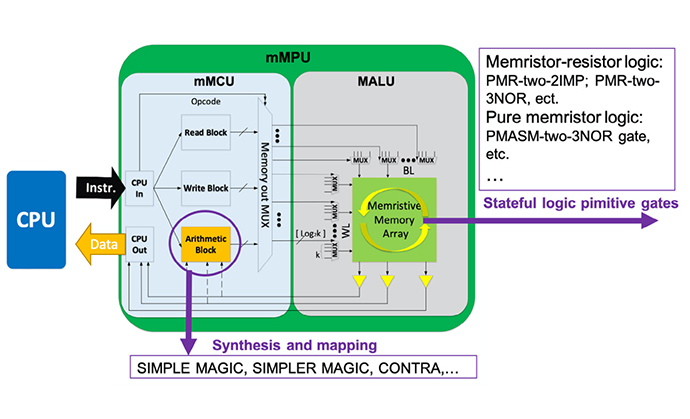
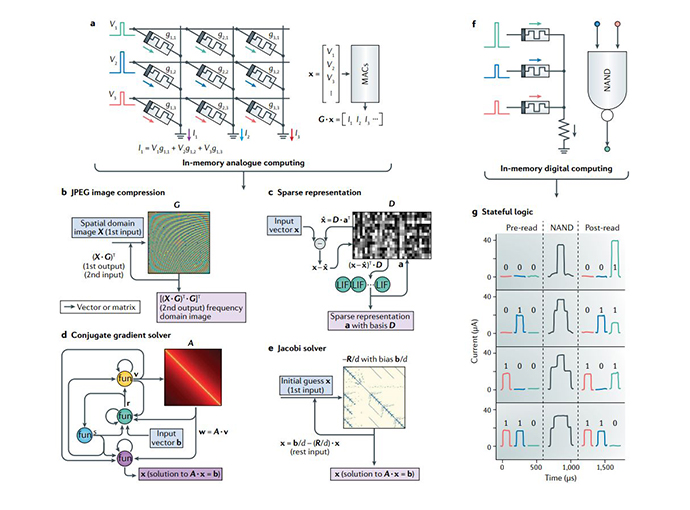
3. Digital & Analog Logic-in-Memory (LIM)
- Modern computing systems are based on von Neumann architecture in which the processor and memory are separated physically. The requirement for data-centric application and the memory wall problem necessitates a new computing architecture.
- Among the research, the emerging technology called in-memory-computing does not require data migration between memory and computing unit, which enhances the computation speed and lowers the energy consumption breaking the memory wall problem. Utilizing the small cell size (4F2) of the resistive switching RAM and the inherent characteristic of the gradual conductance change, digital and analog logic-in-memory computing can be realized.
- Our group focuses on the various types of in-memory computing, such as V-R logic and R-R logic. The scope includes logic device engineering and designing system architecture to improve computation efficiency. The representative work includes a stateful logic based on the primitive circuit of an antiparallel bipolar memristor.
Related Papers :
- N. Xu, T. Park et al. "A Stateful Logic Family Based on a New Logic Primitive Circuit Composed of Two Antiparallel Bipolar Memristors." Adv. Intell. Sys., 190082 (2019).
- Z. Wang et al. "Resistive switching materials for information processing." Nature Review Materials, 5 (2020).
- N. Xu, T. Park et al. "In-Memory Stateful Logic Computing Using Memristors: Gate, Calculation, and Application." Phys. Status Solidi RRL, 2100208 (2021).
- T. Park et al. "Reliable Domain-Specific Exclusive Logic Gates Using Reconfigurable Sequential Logic Based on Antiparallel Bipolar Memristors." Advanced Intelligent Systems, 2100267 (2022).